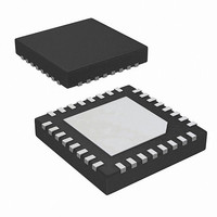
ISL9440BIRZ-T Intersil, ISL9440BIRZ-T Datasheet - Page 18

ISL9440BIRZ-T
Manufacturer Part Number
ISL9440BIRZ-T
Description
IC CTRLR PWM OUT-OF-PHASE 32-QFN
Manufacturer
Intersil
Datasheet
1.ISL9440BIRZ.pdf
(24 pages)
Specifications of ISL9440BIRZ-T
Pwm Type
Current Mode
Number Of Outputs
4
Frequency - Max
340kHz
Duty Cycle
93%
Voltage - Supply
4.5 V ~ 24 V
Buck
Yes
Boost
No
Flyback
No
Inverting
No
Doubler
No
Divider
No
Cuk
No
Isolated
No
Operating Temperature
-40°C ~ 85°C
Package / Case
32-VQFN Exposed Pad, 32-HVQFN, 32-SQFN, 32-DHVQFN
Frequency-max
340kHz
Lead Free Status / RoHS Status
Lead free / RoHS Compliant
Available stocks
Company
Part Number
Manufacturer
Quantity
Price
Company:
Part Number:
ISL9440BIRZ-T
Manufacturer:
Intersil
Quantity:
6 000
shielding requirements for EMI. The typical operating curves
show the synchronized 180° out-of-phase operation.
Input Voltage Range
The ISL9440B and ISL9440C are designed to operate from
input supplies ranging from 4.5V to 24V.
For 5V ±10% input applications, the ISL9441 is suggested.
The reason is that V
together for this input application. The early warning function
will pull PGOOD and RST low for ISL9440B and ISL9440C.
The input voltage range can be effectively limited by the
available maximum duty cycle (D
and D
Where:
V
discharge path, including the lower FET, inductor and PC
board.
V
including the upper FET, inductor and PC board resistances.
The maximum input voltage and minimum output voltage is
limited by the minimum ON-time (t
where, t
Gate Control Logic
The gate control logic translates generated PWM signals into
gate drive signals providing amplification, level shifting and
shoot-through protection. The gate drivers have some circuitry
that helps optimize the IC performance over a wide range of
operational conditions. As MOSFET switching times can vary
dramatically from type to type and with input voltage, the gate
control logic provides adaptive dead-time by monitoring real
gate waveforms of both the upper and the lower MOSFETs.
Shoot-through control logic provides a 20ns dead-time to
ensure that both the upper and lower MOSFETs will not turn on
simultaneously and cause a shoot-through condition.
Gate Drivers
The low-side gate driver is supplied from VCC_5V and
provides a peak sink current of 2A/2A/200mA and source
current of 800mA/800mA/400mA for Channels 1, 2, 3
respectively. The high-side gate driver is also capable of
delivering the same current as those in low-side gate driver.
Gate-drive voltages for the upper N-Channel MOSFET are
generated by the flying capacitor boot circuit. A boot capacitor
connected from the BOOT pin to the PHASE node provides
power to the high-side MOSFET driver. To limit the peak
current in the IC, an external resistor may be placed between
the UGATE pin and the gate of the external MOSFET. This
small series resistor also damps any oscillations caused by
V
V
IN min
d1
d2
IN max
(
= Sum of the parasitic voltage drops in the inductor
= Sum of the voltage drops in the charging path,
(
MAX
)
ON(min)
)
=
≤
= 86% for ISL9440C), as shown in Equation 3.
⎛
⎝
--------------------------------------------------- -
t
ON min
V
--------------------------------
OUT
(
= 30ns
0.93
V
+
OUT
)
V
×
IN
d1
300kHz
and VCC_5V Pin should be tied
⎞
⎠
+
V
d2
18
–
V
MAX
d1
ON(min)
= 93% for ISL9440B,
).(see Equation 4).
ISL9440B, ISL9440C
(EQ. 3)
(EQ. 4)
the resonant tank of the parasitic inductances in the traces of
the board and the FET’s input capacitance.
At start-up, the low-side MOSFET turns on and forces
PHASE to ground in order to charge the BOOT capacitor to
5V. After the low-side MOSFET turns off, the high-side
MOSFET is turned on by closing an internal switch between
BOOT and UGATE. This provides the necessary
gate-to-source voltage to turn on the upper MOSFET, an
action that boosts the 5V gate drive signal above VIN. The
current required to drive the upper MOSFET is drawn from
the internal 5V regulator.
Adaptive Dead Time
The ISL9440B and ISL9440C incorporate an adaptive
dead-time algorithm on the synchronous buck PWM
controllers that optimizes operation with varying MOSFET
conditions. This algorithm provides an approximately 20ns of
dead-time between switching the upper and lower
MOSFETs. This dead time is adaptive and allows operation
with different MOSFETs without having to externally adjust
the dead-time using a resistor or capacitor. During turn-off of
the lower MOSFET, the LGATE voltage is monitored until it
reaches a 1V threshold, at which time the UGATE is
released to rise. Adaptive dead time circuitry monitors the
upper MOSFET gate voltage during UGATE turn-off. Once
the upper MOSFET gate-to-source voltage has dropped
below a threshold of 1V, the LGATE is allowed to rise.
Internal Bootstrap Diode
The ISL9440B and ISL9440C have integrated bootstrap
diodes to help reduce total cost and reduce layout
complexity. Simply adding an external capacitor across the
BOOT and PHASE pins completes the bootstrap circuit. The
bootstrap capacitor must have a maximum voltage rating
above the maximum battery voltage plus 5V. The bootstrap
capacitor can be chosen from Equation 5.
C
BOOT
≥
----------------------- -
ΔV
Q
GATE
BOOT
ISL9440B
UGATE
PHASE
VCC_5V
BOOT
FIGURE 41.
VIN
June 24, 2010
(EQ. 5)
FN6799.3


