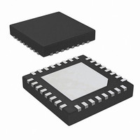
ISL9440BIRZ-T Intersil, ISL9440BIRZ-T Datasheet - Page 21

ISL9440BIRZ-T
Manufacturer Part Number
ISL9440BIRZ-T
Description
IC CTRLR PWM OUT-OF-PHASE 32-QFN
Manufacturer
Intersil
Datasheet
1.ISL9440BIRZ.pdf
(24 pages)
Specifications of ISL9440BIRZ-T
Pwm Type
Current Mode
Number Of Outputs
4
Frequency - Max
340kHz
Duty Cycle
93%
Voltage - Supply
4.5 V ~ 24 V
Buck
Yes
Boost
No
Flyback
No
Inverting
No
Doubler
No
Divider
No
Cuk
No
Isolated
No
Operating Temperature
-40°C ~ 85°C
Package / Case
32-VQFN Exposed Pad, 32-HVQFN, 32-SQFN, 32-DHVQFN
Frequency-max
340kHz
Lead Free Status / RoHS Status
Lead free / RoHS Compliant
Available stocks
Company
Part Number
Manufacturer
Quantity
Price
Company:
Part Number:
ISL9440BIRZ-T
Manufacturer:
Intersil
Quantity:
6 000
The linear regulator output can be supplied by the output of
one of the PWMs. When using a PFET, the output of the
linear regulator will track the PWM supply after the PWM
output rises to a voltage greater than the threshold of the
PFET pass device. The voltage differential between the
PWM and the linear output will be the load current times the
r
Base-Drive Noise Reduction
The high-impedance base driver is susceptible to system
noise, especially when the linear regulator is lightly loaded.
Capacitively coupled switching noise or inductively coupled
EMI onto the base drive causes fluctuations in the base
current, which appear as noise on the linear regulator’s
output. Keep the base drive traces away from the step-down
converter, and as short as possible, to minimize noise
coupling. A resistor in series with the gate drivers reduces
the switching noise generated by PWM. Additionally, a
bypass capacitor may be placed across the base-to-emitter
resistor. This bypass capacitor, in addition to the transistor’s
input capacitor, could bring in a second pole that will
destabilize the linear regulator. Therefore, the stability
requirements determine the maximum base-to-emitter
capacitance.
Layout Guidelines
Careful attention to layout requirements is necessary for
successful implementation of an ISL9440B and ISL9440C
based DC/DC converter. The ISL9440B and ISL9440C
switch at a very high frequency and therefore, the switching
times are very short. At these switching frequencies, even
the shortest trace has significant impedance. Also, the peak
gate drive current rises significantly in an extremely short
time. Transition speed of the current from one device to
another causes voltage spikes across the interconnecting
impedances and parasitic circuit elements. These voltage
spikes can degrade efficiency, generate EMI, increase
device overvoltage stress and ringing. Careful component
selection and proper PC board layout minimizes the
magnitude of these voltage spikes.
There are three sets of critical components in a DC/DC
converter using the ISL9440B and ISL9440C: the controller,
the switching power components and the small signal
components. The switching power components are the most
critical from a layout point of view because they switch a
large amount of energy so they tend to generate a large
amount of noise. The critical small signal components are
those connected to sensitive nodes or those supplying
critical bias currents. A multi-layer printed circuit board is
recommended.
Layout Considerations
DS(ON)
1. The Input capacitors, Upper FET, Lower FET, Inductor
and Output capacitor should be placed first. Isolate these
power components on the topside of the board with their
ground terminals adjacent to one another. Place the input
.
21
ISL9440B, ISL9440C
10. Route all high speed switching nodes away from the
11. Create a separate small analog ground plane near the IC.
12. Separate current sensing traces from PHASE node
13. Ensure the feedback connection to the output capacitor is
Component Selection Guidelines
MOSFET Considerations
The logic level MOSFETs are chosen for optimum efficiency
given the potentially wide input voltage range and output
power requirements. Two N-Channel MOSFETs are used in
each of the synchronous-rectified buck converters for the 3
PWM outputs. These MOSFETs should be selected based
upon r
management considerations.
2. Use separate ground planes for power ground and small
3. The loop formed by Input capacitor, the top FET and the
4. Ensure the current paths from the input capacitor to the
5. Place The PWM controller IC close to lower FET. The
6. Place VCC_5V bypass capacitor very close to VCC_5V
7. Place the gate drive components BOOT diode and BOOT
8. The output capacitors should be placed as close to the
9. Use copper filled polygons or wide but short trace to
high frequency decoupling ceramic capacitor very close
to the MOSFETs.
signal ground. Connect the SGND and PGND together
close to the IC. Do not connect them together anywhere
else.
bottom FET must be kept as small as possible.
MOSFET, to the output inductor and output capacitor are
as short as possible with maximum allowable trace
widths.
LGATE connection should be short and wide. The IC can
be best placed over a quiet ground area. Avoid switching
ground loop current in this area.
pin of the IC and connect its ground to the PGND plane.
capacitors together near controller IC.
load as possible. Use short wide copper regions to
connect output capacitors-to-load to avoid inductance
and resistances.
connect the junction of upper FET, Lower FET and output
inductor. Also keep the PHASE node connection to the IC
short. Do not unnecessarily oversize the copper islands
for PHASE node. Since the phase nodes are subjected to
very high dv/dt voltages, the stray capacitor formed
between these islands and the surrounding circuitry will
tend to couple switching noise.
control circuitry.
Connect the SGND pin to this plane. All small signal
grounding paths including feedback resistors, current
limit setting resistors and ENx pull-down resistors should
be connected to this SGND plane.
connections
short and direct.
DS(ON)
, gate supply requirements, and thermal
June 24, 2010
FN6799.3


