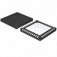
ISL6326BIRZ Intersil, ISL6326BIRZ Datasheet - Page 13

ISL6326BIRZ
Manufacturer Part Number
ISL6326BIRZ
Description
IC CTRLR PWM 4PHASE BUCK 40-QFN
Manufacturer
Intersil
Datasheet
1.ISL6326BCRZ.pdf
(30 pages)
Specifications of ISL6326BIRZ
Pwm Type
Voltage Mode
Number Of Outputs
1
Frequency - Max
275kHz
Duty Cycle
25%
Voltage - Supply
4.75 V ~ 5.25 V
Buck
Yes
Boost
No
Flyback
No
Inverting
No
Doubler
No
Divider
No
Cuk
No
Isolated
No
Operating Temperature
-40°C ~ 85°C
Package / Case
40-VFQFN, 40-VFQFPN
Frequency-max
275kHz
Lead Free Status / RoHS Status
Lead free / RoHS Compliant
Equation 7 shows the ratio of the channel current to the
sensed current I
The inductor DCR value will increase as the temperature
increases. Therefore the sensed current will increase as the
temperature of the current sense element increases. In order
to compensate the temperature effect on the sensed current
signal, a Positive Temperature Coefficient (PTC) resistor can
be selected for the sense resistor R
temperature compensation function of ISL6326B should be
utilized. The integrated temperature compensation function
is described in the Temperature Compensation section.
Channel-Current Balance
The sensed current I
together and divided by the number of active channels. The
resulting average current I
total load current. Channel current balance is achieved by
comparing the sensed current of each channel to the
average current to make an appropriate adjustment to the
PWM duty cycle of each channel with Intersil’s patented
current-balance method.
Channel current balance is essential in achieving the
thermal advantage of multiphase operation. With good
current balance, the power loss is equally dissipated over
multiple devices and a greater area.
Voltage Regulation
The compensation network shown in Figure 5 assures that
the steady-state error in the output voltage is limited only to
the error in the reference voltage (output of the DAC) and
offset errors in the OFS current source, remote-sense and
error amplifiers. Intersil specifies the guaranteed tolerance of
the ISL6326B to include the combined tolerances of each of
these elements.
I
SEN
FIGURE 4. SENSE RESISTOR IN SERIES WITH INDUCTORS
=
ISL6326B INTERNAL CIRCUIT
I
L
CURRENT
⋅
SENSE
I
R
-----------------------
SEN
R
SENSE
I
n
ISEN
=
SEN
I L
R SENSE
------------------------- -
.
n
R
from each active channel are summed
ISEN
+
-
AVG
13
provides a measure of the
ISEN-(n)
ISEN+(n)
L
ISEN
R
I
SENSE
L
, or the integrated
R
C
ISEN(n)
T
C
V
OUT
OUT
(EQ. 7)
ISL6326B
The sensed average current I
This current will develop voltage drop across the resistor
between FB and VDIFF pins for droop control. ISL6326B
can not be used for non-droop applications.
The output of the error amplifier, V
sawtooth waveforms to generate the PWM signals. The
PWM signals control the timing of the Intersil MOSFET
drivers and regulate the converter output to the specified
reference voltage. The internal and external circuitry which
control voltage regulation is illustrated in Figure 5.
The ISL6326B incorporates an internal differential remote-
sense amplifier in the feedback path. The amplifier removes
the voltage error encountered when measuring the output
voltage relative to the local controller ground reference point
resulting in a more accurate means of sensing output
voltage. Connect the microprocessor sense pins to the non-
inverting input, VSEN, and inverting input, RGND, of the
remote-sense amplifier. The remote-sense output, V
connected to the inverting input of the error amplifier through
an external resistor.
A digital-to-analog converter (DAC) generates a reference
voltage based on the state of logic signals at pins VID7
through VID0. The DAC decodes the eight 6-bit logic signal
(VID) into one of the discrete voltages shown in Table 1.
Each VID input offers a 45µA pull-up to an internal 2.5V
source for use with open-drain outputs. The pull-up current
diminishes to zero above the logic threshold to protect
voltage-sensitive output devices. External pull-up resistors
can augment the pull-up current sources if case leakage into
the driving device is greater than 45µA.
FIGURE 5. OUTPUT VOLTAGE AND LOAD-LINE
R
FB
EXTERNAL CIRCUIT
V
V
OUT
OUT
+
-
V
DROOP
C
R
REF
-
+
C
REGULATION WITH OFFSET ADJUSTMENT
R
C
REF
C
RGND
COMP
VDIFF
VSEN
DAC
REF
FB
AVG
ISL6326B INTERNAL CIRCUIT
I
AVG
is tied to FB internally.
COMP
DIFFERENTIAL
REMOTE-SENSE
AMPLIFIER
ERROR AMPLIFIER
+
, is compared to
-
+
-
V
COMP
April 21, 2006
DIFF
FN9286.0
, is


