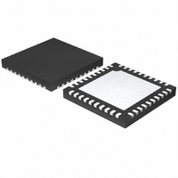
ISL6326BIRZ Intersil, ISL6326BIRZ Datasheet - Page 29

ISL6326BIRZ
Manufacturer Part Number
ISL6326BIRZ
Description
IC CTRLR PWM 4PHASE BUCK 40-QFN
Manufacturer
Intersil
Datasheet
1.ISL6326BCRZ.pdf
(30 pages)
Specifications of ISL6326BIRZ
Pwm Type
Voltage Mode
Number Of Outputs
1
Frequency - Max
275kHz
Duty Cycle
25%
Voltage - Supply
4.75 V ~ 5.25 V
Buck
Yes
Boost
No
Flyback
No
Inverting
No
Doubler
No
Divider
No
Cuk
No
Isolated
No
Operating Temperature
-40°C ~ 85°C
Package / Case
40-VFQFN, 40-VFQFPN
Frequency-max
275kHz
Lead Free Status / RoHS Status
Lead free / RoHS Compliant
Layout Considerations
The following layout strategies are intended to minimize the
impact of board parasitic impedances on converter
performance and to optimize the heat-dissipating capabilities
of the printed-circuit board. These sections highlight some
important practices which should not be overlooked during the
layout process.
Component Placement
Within the allotted implementation area, orient the switching
components first. The switching components are the most
critical because they carry large amounts of energy and tend
to generate high levels of noise. Switching component
placement should take into account power dissipation. Align
the output inductors and MOSFETs such that space between
the components is minimized while creating the PHASE
plane. Place the Intersil MOSFET driver IC as close as
possible to the MOSFETs they control to reduce the parasitic
impedances due to trace length between critical driver input
and output signals. If possible, duplicate the same
placement of these components for each phase.
Next, place the input and output capacitors. Position one
high-frequency ceramic input capacitor next to each upper
MOSFET drain. Place the bulk input capacitors as close to
the upper MOSFET drains as dictated by the component
size and dimensions. Long distances between input
capacitors and MOSFET drains result in too much trace
inductance and a reduction in capacitor performance. Locate
the output capacitors between the inductors and the load,
while keeping them in close proximity to the microprocessor
socket.
FIGURE 20. NORMALIZED INPUT-CAPACITOR RMS
0.6
0.4
0.2
0
0
I
I
I
CURRENT vs DUTY CYCLE FOR SINGLE-PHASE
CONVERTER
L,PP
L,PP
L,PP
0.2
= 0
= 0.5 I
= 0.75 I
O
DUTY CYCLE (V
O
0.4
29
0.6
O/
V
IN
)
0.8
1.0
ISL6326B
April 21, 2006
FN9286.0


