ISL6265HRTZ-T Intersil, ISL6265HRTZ-T Datasheet - Page 11
ISL6265HRTZ-T
Manufacturer Part Number
ISL6265HRTZ-T
Description
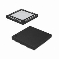
IC CTLR MULTI-OUTPUT 48-TQFN
Manufacturer
Intersil
Datasheet
1.ISL6265HRTZ.pdf
(24 pages)
Specifications of ISL6265HRTZ-T
Applications
Controller, AMD SVI Capable Mobile
Voltage - Input
5 ~ 24 V
Number Of Outputs
3
Voltage - Output
0.5 ~ 1.55 V
Operating Temperature
-10°C ~ 100°C
Mounting Type
Surface Mount
Package / Case
48-TQFN
Lead Free Status / RoHS Status
Lead free / RoHS Compliant


output ripple and lower phase jitter than either conventional
hysteretic or fixed frequency PWM controllers. Unlike
conventional hysteretic converters, the ISL6265 has an error
amplifier that allows the controller to maintain a 0.5% voltage
regulation accuracy throughout the VID range from 0.75V to
1.55V. Voltage regulation accuracy is slightly wider, ±5mV,
over the VID range from 0.7375V to 0.5V.
The hysteresis window voltage is relative to the error
amplifier output such that load current transients result in
increased switching frequency, which gives the R
a faster response than conventional fixed frequency PWM
controllers. In uniplane configurations, transient load current
is inherently shared between active phases due to the use of
a common hysteretic window voltage. Individual average
phase currents are monitored and controlled to equally
share current among the active phases.
Modulator
The ISL6265 modulator features Intersil’s R
hybrid of fixed frequency PWM control and variable
frequency hysteretic control (see Figure 5). Intersil’s R
technology can simultaneously affect the PWM switching
frequency and PWM duty cycle in response to input voltage
and output load transients. The R
AC signal V
output inductor ripple current. The duty-cycle of V
result of charge and discharge current through a ripple
capacitor C
transconductance amplifier g
VO voltages. The positive slope of V
determined by Equation 1:
The negative slope of V
Equation 2:
Where g
A window voltage V
amplifier output voltage V
which the ripple voltage V
V
pins. The V
comparator in which V
and V
PWM pulses being generated as V
V
proportional to the slew rates of the positive and negative
slopes of V
between V
V
V
RPOS
W
COMP
RNEG
is set by a resistor connected across the FSET and GND
W
thresholds. The PWM switching frequency is
=
=
is the higher threshold voltage. Figure 6 shows
m
(
g
is the gain of the transconductance amplifier.
W
g
R;
R
R,
m
R
m
. The current through C
and V
, which is an analog representation of the
⋅
)
it is inversely proportional to the voltage
V
V
⋅
COMP,
(
OUT
V
IN
COMP
W
–
and V
V
is referenced with respect to the error
COMP
OUT
R
.
COMP
can be written as determined by
R
)
W
is compared. The amplitude of
is the lower threshold voltage
m
11
signals feed into a window
, creating an envelope into
that measures the VIN and
3
modulator synthesizes an
R
R
R
traverses the V
is provided by a
can be written as
3
technology, a
3
R
regulator
is the
W
(EQ. 2)
(EQ. 1)
3
and
ISL6265
.
Initialization
Once sufficient bias is applied to the VCC pin, internal logic
checks the status of critical pins to determine the controller
operation profile prior to ENABLE. These pins include RTN1
which determines single vs two-phase operation and
OFS/VFIXEN for enabling/disabling the SVI interface and core
voltage droop. Depending on the configuration set by these
pins, the controller then checks the state of the SVC and SVD
pins to determine the soft-start target output voltage level.
Power-On Reset
The ISL6265 requires a +5V input supply tied to VCC and
PVCC to exceed a rising power-on reset (POR) threshold
before the controller has sufficient bias to guarantee proper
operation. Once this threshold is reached or exceeded, the
ISL6265 has enough bias to begin checking RTN1,
OFS/VFIXEN, ENABLE, and SVI inputs. Hysteresis between
the rising the falling thresholds assure the ISL6265 will not
inadvertently turn-off unless the bias voltage drops
substantially (see “Electrical Specifications” on page 8).
Core Configuration
The ISL6265 determines the core channel requirements of
the CPU based on the state of the RTN1 pin prior to
RIPPLE CAPACITOR VOLTAGE C
FIGURE 6. MODULATOR WAVEFORMS DURING LOAD
VO
VIN
g
+
+
g
-
-
m
m
FIGURE 5. MODULATOR CIRCUITRY
V
TRANSIENT
V
IN
O
ERROR AMPLIFIER VOLTAGE V
+
-
PWM FREQUENCY
CONTROL
C
R
TO
PWM
CONTROL
R
V
V
COMP
V
+
-
R
W
WINDOW VOLTAGE V
+
+
-
-
PWM
PWM
ISL6265
COMP
R
Q
S
May 13, 2009
FN6599.1
FSET
W
Related parts for ISL6265HRTZ-T
Image
Part Number
Description
Manufacturer
Datasheet
Request
R

Part Number:
Description:
Multi-Output Controller
Manufacturer:
Intersil Corporation
Datasheet:
Part Number:
Description:
Intersil Corporation [CMOS Serial Controller Interface]
Manufacturer:
Intersil Corporation
Datasheet:
Part Number:
Description:
Manufacturer:
Intersil Corporation
Datasheet:
Part Number:
Description:
357-036-542-201 CARDEDGE 36POS DL .156 BLK LOPRO
Manufacturer:
Intersil Corporation
Datasheet:
Part Number:
Description:
1024-Word x 4-Bit LSI Static RAM
Manufacturer:
Intersil Corporation
Datasheet:
Part Number:
Description:
General Purpose NPN Transistor Arrays FN341.4
Manufacturer:
Intersil Corporation
Datasheet:
Part Number:
Description:
CMOS 16-Bit Microprocessor
Manufacturer:
Intersil Corporation
Datasheet:
Part Number:
Description:
Manufacturer:
Intersil Corporation
Datasheet:
Part Number:
Description:
Manufacturer:
Intersil Corporation
Datasheet:
Part Number:
Description:
Manufacturer:
Intersil Corporation
Datasheet:
Part Number:
Description:
Manufacturer:
Intersil Corporation
Datasheet:
Part Number:
Description:
CMOS 6-Bit Latch and Decoder Memory Interfaces
Manufacturer:
Intersil Corporation
Datasheet:
Part Number:
Description:
CA3046General Purpose NPN Transistor Arrays
Manufacturer:
Intersil Corporation
Datasheet:
Part Number:
Description:
Manufacturer:
Intersil Corporation
Datasheet:
Part Number:
Description:
TR909 DLC/FLC SLIC with Low Power Standby
Manufacturer:
Intersil Corporation
Datasheet: