ISL6265HRTZ-T Intersil, ISL6265HRTZ-T Datasheet - Page 19
ISL6265HRTZ-T
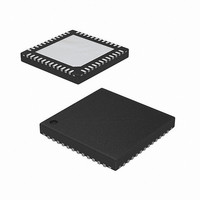
Manufacturer Part Number
ISL6265HRTZ-T
Description
IC CTLR MULTI-OUTPUT 48-TQFN
Manufacturer
Intersil
Datasheet
1.ISL6265HRTZ.pdf
(24 pages)
Specifications of ISL6265HRTZ-T
Applications
Controller, AMD SVI Capable Mobile
Voltage - Input
5 ~ 24 V
Number Of Outputs
3
Voltage - Output
0.5 ~ 1.55 V
Operating Temperature
-10°C ~ 100°C
Mounting Type
Surface Mount
Package / Case
48-TQFN
Lead Free Status / RoHS Status
Lead free / RoHS Compliant


The sense capacitor voltage, V
current rises per Equation 7. When the inductor current rises
to the OC trip level, the voltage across the sense capacitor
will reach a maximum based on the resistor ratio K. This
maximum value, V
compared to the static OC trip level set by the OCSET pin.
The recommended voltage range for V
which sets the resistor divider ratio K, where I
defined OC trip level (see Equation 13). Typical inductor
DCR values are on the order of 1mΩ which result in more
than enough voltage drop to support this V
The resistor divider components also impact time-constant
matching, these components need to meet the parallel
combination requirements of Equation 9.
Based on the selected V
trip level is set. The recommended V
result in an OC monitor trip level range of 30mV to 125mV
based on the internal gain of 5.
This OC monitor trip level sets the voltage level required at
the OCSET pin to create an OC fault at the user-defined OC
trip level. A resistor divider from the RBIAS pin to ground
with the mid-point connected to OCSET sets the voltage at
the pin (see Figure 10). This voltage is internally divided by 6
and compared with V
required at the OCSET pin to achieve this OC trip level
ranges from 180mV to 0.750mV as defined in Equation 14.
The resistor divider ratio used to determine the R
R
K
V
----------------------------------------------- -
R
OC TRIP CURRENT
OCSET
OCSET
OCSET
=
5 x V
R
--------------------------- -
I
OC
OCSET
V
OC
C OC
C(OC)
values is shown in Equation 15.
⋅
(
+
=
DCR
R
V
BIAS
)
@
C OC
(
FIGURE 10. OC TRIP CIRCUITRY
+
-
5x
=
)
V
C(OC)
⋅
OCSET
V
-----------------------
30
1.17V
OCSET
6
C(OC)
CURRENT
SENSE
, is gained up by a factor of 5 and
C(OC)
BIAS
. Working backwards, the voltage
CKT
ISL6265
19
level, the required OC monitor
6
C
, will increase as inductor
OCSET
ISP
C(OC)
ISN
ADDITIONAL DETAIL
R
10µA
SEE FIGURE 9 FOR
BIAS
C,OC
C,OC
level range will
is 6mV to 25mV,
V
+
_
c
1.17V
OC
range.
is the user-
BIAS
R
V
R
OCSET
BIAS
OCSET
(EQ. 13)
(EQ. 14)
(EQ. 15)
and
ISL6265
The resistor values must also meet the R
that the total series resistance to ground equal 117kΩ.
NORTHBRIDGE OC DETECTION
Northbridge OC sensing is achieved via r
across the lower MOSFET. An internal 10µA current source
develops a voltage across R
with the voltage developed across the low-side MOSFET as
measured at the PHASE pin. When the voltage drop across
the MOSFET exceeds the voltage drop across the resistor,
an OC event occurs. The OCSET_NB resistor is selected
based on the relationship in Equation 16.
Where I
application and r
the lower MOSFET.
OC FAULT RESPONSE
When an OC fault occurs on any combination of outputs,
both Core and Northbridge regulators shutdown and the
driver outputs are tri-stated. The PGOOD signal transitions
low indicating a fault condition. The controller will not attempt
to restart the regulators and the user must toggle either EN
or VCC to clear the fault condition.
Overvoltage Protection
The ISL6265 monitors the individual Core and Northbridge
output voltages using differential remote sense amplifiers.
During an OV, PGOOD is latched low and the upper and
lower MOSFETs are turned off on all outputs. Inductor
current will decay through the MOSFET body diodes. This
condition can be reset by bringing EN low or by bringing
VCC below 3.9V. When these inputs are returned to their
high operating levels, the controller soft-starts.
The ISL6265 features a severe overvoltage (OV) threshold
of 1.8V. If any of the outputs exceed this voltage, an OV fault
is immediately triggered. PGOOD is latched low and the
low-side MOSFETs of the offending output(s) are turned on.
The low-side MOSFETs will remain on until the output
voltage is pulled below 0.85V at which time all MOSFETs are
turned off. If the output again rises above 1.8V, the
protection process repeats. This offers protection against a
shorted high-side MOSFET while preventing output voltage
from ringing below ground. The OV is reset by toggling EN
low. OV detection is active at all times that the controller is
enabled including after one of the other faults occurs so that
the processor is protected against high-side MOSFET
leakage while the MOSFETs are commanded off.
Undervoltage Protection
Undervoltage protection is independent of the OC limit. A
fault latches if any of the sensed output voltages are less
than the VID set value by a nominal 295mV for 1ms. The
R
OCSETNB
OC
is the OC trip level selected for the Northbridge
=
I
------------------------------------ -
OC
DS(ON)
10μA
⋅
r
DS ON
(
is the drain-source ON-resistance of
)
OCSET_NB
, which is compared
BIAS
DS(ON)
requirement
sensing
May 13, 2009
(EQ. 16)
FN6599.1
Related parts for ISL6265HRTZ-T
Image
Part Number
Description
Manufacturer
Datasheet
Request
R

Part Number:
Description:
Multi-Output Controller
Manufacturer:
Intersil Corporation
Datasheet:
Part Number:
Description:
Intersil Corporation [CMOS Serial Controller Interface]
Manufacturer:
Intersil Corporation
Datasheet:
Part Number:
Description:
Manufacturer:
Intersil Corporation
Datasheet:
Part Number:
Description:
357-036-542-201 CARDEDGE 36POS DL .156 BLK LOPRO
Manufacturer:
Intersil Corporation
Datasheet:
Part Number:
Description:
1024-Word x 4-Bit LSI Static RAM
Manufacturer:
Intersil Corporation
Datasheet:
Part Number:
Description:
General Purpose NPN Transistor Arrays FN341.4
Manufacturer:
Intersil Corporation
Datasheet:
Part Number:
Description:
CMOS 16-Bit Microprocessor
Manufacturer:
Intersil Corporation
Datasheet:
Part Number:
Description:
Manufacturer:
Intersil Corporation
Datasheet:
Part Number:
Description:
Manufacturer:
Intersil Corporation
Datasheet:
Part Number:
Description:
Manufacturer:
Intersil Corporation
Datasheet:
Part Number:
Description:
Manufacturer:
Intersil Corporation
Datasheet:
Part Number:
Description:
CMOS 6-Bit Latch and Decoder Memory Interfaces
Manufacturer:
Intersil Corporation
Datasheet:
Part Number:
Description:
CA3046General Purpose NPN Transistor Arrays
Manufacturer:
Intersil Corporation
Datasheet:
Part Number:
Description:
Manufacturer:
Intersil Corporation
Datasheet:
Part Number:
Description:
TR909 DLC/FLC SLIC with Low Power Standby
Manufacturer:
Intersil Corporation
Datasheet: