ISL6261AIRZ-T Intersil, ISL6261AIRZ-T Datasheet
ISL6261AIRZ-T
Specifications of ISL6261AIRZ-T


Related parts for ISL6261AIRZ-T


ISL6261AIRZ-T Summary of contents
Page 1
... PART NUMBER (Note) ISL6261ACRZ ISL6261ACRZ-T* ISL6261 ACRZ -10 to +100 40 Ld 6x6 QFN ISL6261AIRZ ISL6261AIRZ-T* 6261A IRZ ® *Please refer to TB347 for details on reel specifications. NOTE: Intersil Pb-free plus anneal products employ special Pb-free material sets; molding compounds/die attach materials and 100% matte tin plate termination finish, which are RoHS compliant and compatible with both SnPb and Pb-free soldering operations ...
Page 2
Pinout FDE PMON RBIAS VR_TT# NTC SOFT OCSET VW COMP FB 2 ISL6261A ISL6261A (40 LD QFN GND PAD (BOTTOM ...
Page 3
... INPUT POWER SUPPLY +5V Supply Current +3.3V Supply Current Battery Supply Current at VIN Pin POR (Power-On Reset) Threshold SYSTEM AND REFERENCES System Accuracy ISL6261ACRZ ISL6261AIRZ RBIAS Voltage Boot Voltage Maximum Output Voltage Minimum Output Voltage VID Off State CHANNEL FREQUENCY Nominal Channel Frequency ...
Page 4
... UGATE to PHASE Resistance GATE DRIVER SWITCHING TIMING (Refer to “Gate Driver Timing Diagram” on page 5) UGATE Turn-on Propagation Delay ISL6261ACRZ ISL6261AIRZ LGATE Turn-on Propagation Delay ISL6261ACRZ ISL6261AIRZ BOOTSTRAP DIODE Forward Voltage Leakage POWER GOOD and PROTECTION MONITOR PGOOD Low Voltage PGOOD Leakage Current ...
Page 5
Electrical Specifications PARAMETER PGOOD Delay Overvoltage Threshold Severe Overvoltage Threshold OCSET Reference Current OC Threshold Offset Undervoltage Threshold (VDIFF-SOFT) LOGIC THRESHOLDS VR_ON and DPRSLPVR Input Low VR_ON and DPRSLPVR Input High Leakage Current on VR_ON ...
Page 6
Functional Pin Description FDE PMON RBIAS VR_TT# NTC SOFT OCSET VW COMP FB FDE Forced diode emulation enable signal. Logic high of FDE with logic low of DPRSTP# forces the ISL6261A to operate in diode emulation mode with an increased ...
Page 7
VSUM This pin is connected to one terminal of the capacitor in the current sensing R-C network. VIN Power stage input voltage used for input voltage feed forward to improve the input line transient performance. VSS Signal ground. ...
Page 8
Function Block Diagram FIGURE 1. SIMPLIFIED FUNCTIONAL BLOCK DIAGRAM OF ISL6261A 8 ISL6261A FN6354.2 December 21, 2007 ...
Page 9
Simplified Application Circuit for DCR Current Sensing VR_TT# VID<0:6> DPRSTP# DPRSLPVR PMON CLK_ENABLE# VR_ON IMVP6_PWRGD VCC-SENSE VSS-SENSE C 3 FIGURE 2. ISL6261A-BASED IMVP-6® SOLUTION WITH INDUCTOR DCR CURRENT SENSING 9 ISL6261A 3V3 ...
Page 10
Simplified Application Circuit for Resistive Current Sensing VR_TT# VID<0:6> DPRSTP# DPRSLPVR PMON CLK_ENABLE# VR_ON IMVP6_PWRGD VCC-SENSE VSS-SENSE FIGURE 3. ISL6261A-BASED IMVP-6® SOLUTION WITH RESISTIVE CURRENT SENSING 10 ISL6261A +3 ...
Page 11
... Emulation Mode (DEM) operation further enhances system efficiency. The heart of the ISL6261A is the patented R Intersil’s Robust Ripple Regulator modulator. The R modulator combines the best features of fixed frequency and hysteretic PWM controllers while eliminating many of their shortcomings. The ISL6261A modulator internally ...
Page 12
TABLE 1. VID TABLE FROM INTEL IMVP-6 SPECIFICATION VID6 VID5 VID4 VID3 VID2 VID1 ...
Page 13
TABLE 1. VID TABLE FROM INTEL IMVP-6 SPECIFICATION (Continued) VID6 VID5 VID4 VID3 VID2 VID1 ...
Page 14
... DPRSTP# and DPRSLPVR logic. Intersil R High-speed input voltage transients have little effect on the output voltage. Intersil R transients to achieve fast response. Upon load application, the ISL6261A will transiently increase the switching frequency to deliver energy to the output more quickly. Compared with steady state operation, the PWM pulses ...
Page 15
Protection The ISL6261A provides overcurrent (OC), overvoltage (OV), undervoltage (UV) and over-temperature (OT) protections as shown in Table 3. Overcurrent is detected through the droop voltage, which is designed as described in the “Component Selection and Application” section. The OCSET ...
Page 16
OC INTERNAL TO ISL6261A DROOP 1 1 VDIFF FIGURE 6. SIMPLIFIED VOLTAGE DROOP CIRCUIT WITH CPU-DIE VOLTAGE SENSING AND INDUCTOR DCR CURRENT SENSING ® The IMVP-6 specification reveals the critical timing associated with regulating the output voltage. SLEWRATE, ® ...
Page 17
These traces should be laid out as noise sensitive traces. For optimum load line regulation performance, the traces connecting these two pins to the Kelvin sense leads of the processor should be laid out away from rapidly rising voltage nodes ...
Page 18
The NTC thermistor’s resistance is approximately given by the following formula: 1 ⋅ − ⋅ 273 NTC NTCTo T is the temperature of the NTC thermistor and b ...
Page 19
... where G network set to n temperature characteristics For different G1 and NTC thermistor preference, Intersil provides a design spreadsheet to generate the proper value of R (EQ. 16) ntc R drp1 droop amplifier gain, according to Equation 22: k droopamp dcr R series R par R ntc ...
Page 20
After determining R and R networks, use Equation calculate the droop resistances R drp1 R droop = − ⋅ drp drp ⋅ DCR ...
Page 21
... It is highly recommended to design the compensation such that the regulator output impedance is 2.1mΩ. A type-III compensator is recommended to achieve the best performance. Intersil provides a spreadsheet to design the compensator parameters. Figure 13 shows an example of the spreadsheet. After the user inputs the parameters in the blue font, the spreadsheet will calculate ...
Page 22
ISL6261A FIGURE 13. AN EXAMPLE OF ISL6261A COMPENSATION SPREADSHEET 22 FN6354.2 December 21, 2007 ...
Page 23
OC Internal to ISL6261A 1 FIGURE 14. EQUIVALENT MODEL FOR DROOP CIRCUIT USING DISCRETE RESISTOR SENSING Typical Performance (ISL6261 Data, Taken on ISL6261A Eval1 Rev.A Evaluation Board) FIGURE 15. CCM EFFICIENCY, VID = 1.1V 8V ...
Page 24
Typical Performance (ISL6261 Data, Taken on ISL6261A Eval1 Rev.A Evaluation Board) (Continued) FIGURE 19. ENHANCED DEM EFFICIENCY, VID = 0.7625V 8V 12.6V AND V IN1 IN2 FIGURE 21. ENHANCED DEM EFFICIENCY, VID = 1.1V ...
Page 25
Typical Performance (ISL6261 Data, Taken on ISL6261A Eval1 Rev.A Evaluation Board) (Continued) 5V/div 0.1V/div 1V/div 10V/div FIGURE 25 VID 19V 2A, VID = 1.5V, BOOT IN Ch1: CLK_EN#, Ch2 Ch3: PMON, O ...
Page 26
Typical Performance (ISL6261 Data, Taken on ISL6261A Eval1 Rev.A Evaluation Board) (Continued) FIGURE 31. C4 ENTRY/EXIT 12.6V 0.7A, IN HFM/LFM/C4 VID = 1.05V/0.8375V/0.7625V, FDE = DPRSLPVR, Ch1: PMON, Ch2: V Ch3: 40k/100pF FILTERED PMON, Ch4: PHASE ...
Page 27
... Accordingly, the reader is cautioned to verify that data sheets are current before placing orders. Information furnished by Intersil is believed to be accurate and reliable. However, no responsibility is assumed by Intersil or its subsidiaries for its use; nor for any infringements of patents or other rights of third parties which may result from its use ...
Page 28
ISL6261A Eval1 Evaluation Board Schematics Controller S1 J8 +3.3V DPRSLPVR PSI R108 4 ON PMON/PGD_IN DNP DPRSTP# SD05H0SK ...
Page 29
ISL6261A Eval1 Evaluation Board Schematics Power Stage VIN IRF7821 IRF7821 UGATE R48 C1 BOOT IN 0 0.22UF PHASE IN IRF7832 IRF7832 LGATE (Continued) 1 OUT 0.45UH 1 J20 4 2 ...
Page 30
ISL6261A Eval1 Evaluation Board Schematics Socket B26 VCCA G21 VCCSENSE VCCP AF7 J6 VCCSENSE VCCP OUT J21 VCCP A7 K6 VCC VCCP IN A9 K21 VCC VCCP A10 M6 VCC VCCP A12 M21 VCORE VCC VCCP A13 N6 VCC VCCP ...
Page 31
ISL6261A Eval1 Evaluation Board Schematics Dynamic Load GND_POWER +12V U5 C80 1 VDD 1UF HIP2100 +12V +12V R72 2N7002 499 1 Q14 (Continued VSS 6 LI R74 5 HI 249 R73 ...
Page 32
ISL6261A Eval1 Evaluation Board Schematics Geyserville Transition Gen ...
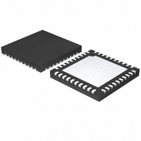
Page 33
Package Outline Drawing L40.6x6 40 LEAD QUAD FLAT NO-LEAD PLASTIC PACKAGE Rev 3, 10/06 6.00 6 PIN 1 INDEX AREA (4X) 0.15 TOP VIEW ( TYP ) ( TYPICAL RECOMMENDED LAND PATTERN 33 ...