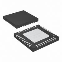
MAX8720ETX+ Maxim Integrated Products, MAX8720ETX+ Datasheet - Page 15

MAX8720ETX+
Manufacturer Part Number
MAX8720ETX+
Description
IC CNTRL VID STP DWN 36-TQFN
Manufacturer
Maxim Integrated Products
Datasheet
1.MAX8720ETXT.pdf
(31 pages)
Specifications of MAX8720ETX+
Applications
Controller, CPU GPU
Voltage - Input
2 ~ 28 V
Number Of Outputs
1
Voltage - Output
0.28 ~ 1.85 V
Operating Temperature
0°C ~ 85°C
Mounting Type
Surface Mount
Package / Case
36-TQFN Exposed Pad
Output Voltage
0.275 V to 1.85 V
Input Voltage
2 V to 28 V
Mounting Style
SMD/SMT
Maximum Operating Temperature
+ 85 C
Minimum Operating Temperature
- 40 C
Lead Free Status / RoHS Status
Lead free / RoHS Compliant
dynamic output-voltage transitions when the inductor
current reverses at light or negative load currents. With
reversed inductor current, the inductor’s EMF causes LX
to go high earlier than normal, extending the on-time by
a period equal to the DH-rising dead time.
For loads above the critical conduction point, where the
dead-time effect is no longer a factor, the actual switch-
ing frequency is:
where V
the inductor discharge path, including synchronous
rectifier, inductor, and PC board resistances; V
the sum of the parasitic voltage drops in the inductor
charge path, including high-side switch, inductor, and
PC board resistances; and t
ed by the MAX8720.
Three integrator amplifiers provide a fine adjustment to
the output regulation point. One amplifier integrates the
difference between GNDS and AGND, and a second
integrates the difference between FBS and FB. The
third amplifier integrates the difference between REF
and the DAC output. These three transconductance
amplifiers’ outputs are directly summed inside the chip,
so the integration time constant can be set easily with
one capacitor. The G
The integrator block has the ability to lower the output
voltage by 2% and raise it by 6%. For each amplifier,
the differential input voltage range is at least ±70mV
total, including DC offset and AC ripple. The integrator
corrects for approximately 90% of the total error, due to
finite gain.
The FBS amplifier corrects for DC voltage drops in PC
board traces and connectors in the output bus path
between the DC-DC converter and the load. The GNDS
amplifier performs a similar DC correction task for the
output ground bus. The third integrator amplifier cor-
rects the small offset of the error amplifier and provides
an averaging function that forces V
at the average value of the output ripple waveform.
Integrators have both beneficial and detrimental charac-
teristics. Although they correct for drops due to DC bus
resistance and tighten the DC output-voltage tolerance
limits by averaging the peak-to-peak output ripple, they
can interfere with achieving the fastest possible load-
transient response. The fastest transient response is
achieved when all three integrators are disabled.
DIS
is the sum of the parasitic voltage drops in
f
SW
=
______________________________________________________________________________________
t
ON IN
m
(
Integrator Amplifiers and
V
of each amplifier is 160µS (typ).
V
OUT
Output-Voltage Offsets
+
V
ON
DIS
+
V
is the on-time calculat-
DIS
−
V
OUT
Dynamically Adjustable 6-Bit VID
CHG
to be regulated
)
CHG
is
This can work very well if the MAX8720 circuit is placed
very close to the CPU. All three integrators can be dis-
abled by connecting FBS to V
are disabled, CC can be left unconnected, which elimi-
nates a component but leaves GNDS connected to any
convenient ground. When the inductor is in continuous
conduction, the output voltage has a DC regulation high-
er than the trip level by 50% of the ripple. In discontinu-
ous conduction (SKIP = GND, light loaded), the output
voltage has a DC regulation higher than the trip level by
approximately 1.5% due to slope compensation.
There is often a connector, or at least many milliohms of
PC board trace resistance, between the DC-DC con-
verter and the CPU. In these cases, the best strategy is
to place most of the bulk bypass capacitors close to
the CPU, with just one capacitor on the other side of the
connector near the MAX8720 to control ripple if the
CPU card is unplugged. In this situation, the remote-
sense lines (GNDS and FBS) and integrators provide a
real benefit.
The low-noise forced-PWM mode (SKIP = high) dis-
ables the zero-crossing comparator, allowing the
inductor current to reverse at light loads. This causes
the low-side gate-drive waveform to become the com-
plement of the high-side gate-drive waveform. The ben-
efit of forced-PWM mode is to keep the switching
frequency fairly constant, but it comes at a cost: the no-
load battery current can be 10mA to 40mA, depending
on the external MOSFETs and switching frequency.
Forced-PWM mode is required during downward out-
put-voltage transitions. The MAX8720 uses PWM mode
during all transitions, but only while the slew-rate con-
troller is active. Due to voltage positioning, when a tran-
sition uses high negative inductor current, the output
voltage does not settle to its final intended value until
well after the slew-rate controller terminates. Because
of this it is possible, at very high negative slew currents,
for the output to end up high enough to cause PGOOD
to go low.
Thus, it is necessary to use forced-PWM mode during all
negative transitions. Most applications should use PWM
mode exclusively, although there is some benefit to
using skip mode while in the low-power suspend state.
In skip mode (SKIP = GND), an inherent automatic
switchover to PFM takes place at light loads (Figure 3).
This switchover is affected by a comparator that trun-
cates the low-side switch on-time at the inductor cur-
rent’s zero crossing. This mechanism causes the
Step-Down Controller
Automatic Pulse-Skipping Switchover
Forced-PWM Mode (
CC
. When the integrators
( SKIP = GND)
SKIP = High)
15


