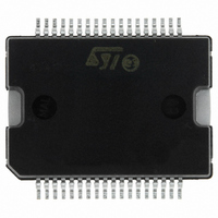
L6701 STMicroelectronics, L6701 Datasheet - Page 30

L6701
Manufacturer Part Number
L6701
Description
IC CTRLR 3PH VR10/9/K8 PWRSO-36
Manufacturer
STMicroelectronics
Datasheet
1.L6701TR.pdf
(44 pages)
Specifications of L6701
Applications
Controller, Intel VR9, VR10, K8
Voltage - Input
12V
Number Of Outputs
3
Voltage - Output
0.8 ~ 1.85 V
Operating Temperature
0°C ~ 70°C
Mounting Type
Surface Mount
Package / Case
36-PowerSOIC
Output Voltage
0.8 V to 1.85 V
Output Current
1.5 A
Switching Frequency
110 KHz
Mounting Style
SMD/SMT
Maximum Operating Temperature
+ 125 C
Minimum Operating Temperature
0 C
Lead Free Status / RoHS Status
Lead free / RoHS Compliant
Available stocks
Company
Part Number
Manufacturer
Quantity
Price
13 Output voltage Monitor and Protections
13.3
13.4
30/44
Figure 13. Output Voltage Protections and typical principle connections
Over Voltage
Once VCC crosses the turn-ON threshold and the device is enabled (EN = Free), L6701
provides an Over Voltage Protection according to the DAC_SEL status: when the voltage
sensed by VSEN overcomes the OVP threshold, the controller permanently switches on all the
low-side MOSFETs and switches off all the high-side MOSFETs in order to protect the load.
The FAULT pin is driven high (5V) and power supply or EN pin cycling is required to restart
operations.
The OVP (and Pre-OVP) Threshold varies according to the operative mode selected as
reported in
Table 10.
Feedback Disconnection
L6701 allows to monitor the output voltage in two different points:
By comparing the voltage present at these two different locations, L6701 is able to understand
if the output voltage feedback is connected. When CS- is more than 1V higher than VSEN,
(See
drives high the FAULT pin. The condition is latched until VCC or EN cycled.
UVLO
UVLO
Remotely, through the remote buffer, across VSEN
Locally across the CS- pin (negligibly offset by
82kΩ to SGND
Figure
VCC
OVP
DAC_SEL
V cc
Open
0
Table
OVP and Preliminary OVP Thresholds
14) the device stops switching with the low side MOSFETs permanently ON and
FBR/DACSEL Monitor
Preliminary OVP
10.
(EN = 0)
Preliminary OVP Enabled
FBR Monitored
No Protection
Provided
Operative Mode
VSEN Monitored
OVP Protection
VR10
VR9
K8
(EN = Free)
+5V
R
+12V
D
⋅
SB
Pre-OVP
I
C S
2.1
1.9
1.9
).
OVP
2.1
1.9
1.9
VCC
L6701


