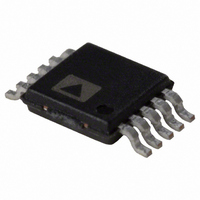
ADP1621ARMZ-R7 Analog Devices Inc, ADP1621ARMZ-R7 Datasheet - Page 12

ADP1621ARMZ-R7
Manufacturer Part Number
ADP1621ARMZ-R7
Description
IC CTRLR DC/DC PWM STEPUP 10MSOP
Manufacturer
Analog Devices Inc
Type
Step-Up (Boost)r
Datasheet
1.ADP1621ARMZ-R7.pdf
(32 pages)
Specifications of ADP1621ARMZ-R7
Internal Switch(s)
No
Synchronous Rectifier
Yes
Number Of Outputs
1
Current - Output
1A
Frequency - Switching
100kHz ~ 1.5MHz
Voltage - Input
2.9 ~ 5.5 V
Operating Temperature
-40°C ~ 125°C
Mounting Type
Surface Mount
Package / Case
10-MSOP, Micro10™, 10-uMAX, 10-uSOP
Primary Input Voltage
5.5V
No. Of Outputs
1
Output Current
1A
No. Of Pins
10
Operating Temperature Range
-40°C To +125°C
Msl
MSL 1 - Unlimited
Frequency Max
1.5MHz
Termination Type
SMD
Lead Free Status / RoHS Status
Lead free / RoHS Compliant
For Use With
ADP1621-EVALZ - BOARD EVALUATION FOR ADP1621
Voltage - Output
-
Power - Output
-
Lead Free Status / RoHS Status
Lead free / RoHS Compliant, Lead free / RoHS Compliant
Other names
ADP1621ARMZ-R7
ADP1621ARMZ-R7TR
ADP1621ARMZ-R7TR
ADP1621
THEORY OF OPERATION
The ADP1621 is a fixed-frequency, current-mode, step-up dc/dc
converter controller. It drives an external n-channel MOSFET
to step the input voltage up to a higher output voltage. It can be
used for SEPIC, flyback, boost, buck-boost, forward, and other
converter topologies. It operates at a fixed switching frequency that
is set by an external resistor over a range of 100 kHz to 1.5 MHz,
and it can be synchronized to an external clock by connecting
the SDSN pin to the clock.
The input supply current to the ADP1621 is less than 3 mA
during normal operation and less than 10 μA during shutdown.
The ADP1621 can drive large external MOSFETs, allowing it to
support load currents in excess of 10 A.
CONTROL LOOP
The ADP1621 uses a current-mode architecture to regulate the
output voltage. The output voltage is monitored at FB through
a resistive voltage divider. The voltage at FB is compared to the
internal 1.215 V reference voltage by the internal transconductance
error amplifier to create an error current at COMP. A resistor-
capacitor compensation impedance connected from COMP to
GND converts the error current to an error voltage.
At the beginning of the switching cycle, the MOSFET is turned
on and the inductor current ramps up. The MOSFET current is
measured and converted to a voltage using R
added to the stabilizing slope-compensation ramp. The resulting
voltage sum passes through the current-sense amplifier to generate
the current-sense voltage. When the current-sense voltage is
greater than the COMP error voltage, the MOSFET is turned off
and the inductor current ramps down until the internal clock
initiates the next switching cycle. The duty-cycle of the PWM
modulator is thus adjusted to provide the necessary load current
at the desired output voltage. Because the output voltage ultimately
controls the peak inductor current through the COMP error
voltage, this scheme is referred to as peak current-mode control.
With light loads, the converter can also operate under discon-
tinuous conduction mode and pulse-skipping modulation to
maintain output-voltage regulation. These two forms of operation
are discussed in detail in the Light Load Operation section.
Note that the converter can also be designed to operate in
discontinuous conduction mode at full load if desired.
Overall, the current-mode regulation system of the ADP1621
allows fast transient responses while maintaining a stable output
voltage. By selecting the proper resistor-capacitor network from
COMP to GND, the regulator response can be optimized for a
wide range of input voltages, output voltages, and load currents.
CS
or R
DSON
and is
Rev. A | Page 12 of 32
CURRENT-SENSE CONFIGURATIONS
The ADP1621 can sense the current across the on resistance of
the MOSFET to minimize external component count and improve
efficiency by eliminating the power that would be lost in a current-
sense resistor. This lossless technique eliminates the need for an
expensive current-sense resistor. In the lossless mode configuration,
the voltage at the CS pin (or the switch-node voltage at the drain of
the MOSFET) must not exceed 30 V (see Figure 28). This technique
maximizes efficiency and reduces cost. In practice, when the
calculated V
measure the actual V
design. Because of the parasitic inductance in the diode, output
capacitor, and PCB traces, V
exceed the theoretical maximum voltage at V
V
peak voltage exceeds 30 V, or if a more accurate current limit is
desired, then the CS pin can be connected to an external current-
sense resistor in the source of the MOSFET (Figure 29). The
maximum power output is limited by the selection of the
external components.
OUT
and the forward-voltage drop of Diode D1. If the measured
Figure 29. CS Pin Connection for V
Figure 28. CS Pin Connection for V
V
V
SW
IN
IN
approaches 30 V, one should build the board and
(No Current-Sense Resistor Needed)
with a Current-Sense Resistor, R
SDSN
SDSN
SW
PGND
PGND
ADP1621
ADP1621
PIN
PIN
before committing to the lossless mode
SW
GND
GND
GATE
GATE
IN
IN
CS
CS
typically has narrow peaks that
SW
> 30 V, Resistor Sense Mode
L
L
R
SW
R
S
S
V
< 30 V, Lossless Mode
SW
V
R
D1
D1
SW
CS
CS
SW
V
V
OUT
OUT
—the sum of
C
C
O
O


