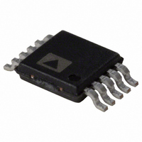
ADP1621ARMZ-R7 Analog Devices Inc, ADP1621ARMZ-R7 Datasheet - Page 25

ADP1621ARMZ-R7
Manufacturer Part Number
ADP1621ARMZ-R7
Description
IC CTRLR DC/DC PWM STEPUP 10MSOP
Manufacturer
Analog Devices Inc
Type
Step-Up (Boost)r
Datasheet
1.ADP1621ARMZ-R7.pdf
(32 pages)
Specifications of ADP1621ARMZ-R7
Internal Switch(s)
No
Synchronous Rectifier
Yes
Number Of Outputs
1
Current - Output
1A
Frequency - Switching
100kHz ~ 1.5MHz
Voltage - Input
2.9 ~ 5.5 V
Operating Temperature
-40°C ~ 125°C
Mounting Type
Surface Mount
Package / Case
10-MSOP, Micro10™, 10-uMAX, 10-uSOP
Primary Input Voltage
5.5V
No. Of Outputs
1
Output Current
1A
No. Of Pins
10
Operating Temperature Range
-40°C To +125°C
Msl
MSL 1 - Unlimited
Frequency Max
1.5MHz
Termination Type
SMD
Lead Free Status / RoHS Status
Lead free / RoHS Compliant
For Use With
ADP1621-EVALZ - BOARD EVALUATION FOR ADP1621
Voltage - Output
-
Power - Output
-
Lead Free Status / RoHS Status
Lead free / RoHS Compliant, Lead free / RoHS Compliant
Other names
ADP1621ARMZ-R7
ADP1621ARMZ-R7TR
ADP1621ARMZ-R7TR
Low Input and High Output Boost Converter
Figure 36 shows a typical application boost converter circuit
that operates at a switching frequency of 200 kHz with V
and V
is about 83%. A higher switching frequency can be selected, but
the switching power loss in the MOSFET increases and a bigger
MOSFET is needed. For switch-node voltages greater than 30 V,
a sense resistor, R
voltage at CS is 33 V.
High Input Voltage Boost Converter Circuit
Input voltages higher than 5.5 V are possible with the addition
of a resistor and an NPN transistor, as shown in Figure 37, or just
OUT
= 30 V with a 1 A load. The duty cycle for this circuit
CS
, is needed because the absolute maximum
120pF
120pF
f
C1 = MURATA GRM31CR60J476M
C
C
C
f
C1 = MURATA GRM32ER61C226K
C
C
C
OSC
OSC
OUT1
OUT2
OUT3
OUT1
OUT2
OUT3
1µF
10V
C3
C2
C2
= 200kHz
= 560kHz
= MURATA GRM31CR72A10
= MURATA GRM55ER71H475K
= RUBYCON 50ZL330M10x23
= MURATA GRM31CR72A105K
= MURATA GRM55ER71H475K
= RUBYCON 50ZL220M10x23
0.1µF
0.1µF
10V
R
1.6MΩ
10V
R
2MΩ
C4
C
20pF
C4
C
220pF
COMP
COMP
COMP
COMP
Figure 37. High Input Voltage and High Output Voltage Converter
R
100kΩ
1%
R
34.8kΩ
Figure 36. Low Input, High Output Boost Converter
FREQ
FREQ
700Ω
SDSN
COMP
FREQ
SDSN
COMP
FREQ
R3
ADP1621
ADP1621
AGND
AGND
IN
IN
IN
= 5 V
GND
GND
PGND
PGND
M1 = VISHAY SUD50N06-07L
D1 = IRF 15TQ060
L1 = COILCRAFT DO501DH-782ML
M1 = IRF7470
Q1 = SIGNAL NPN TRANSISTOR
D1 = MBRB7H50
L1 = COILCRAFT MSS1260-822ML
GATE
GATE
Rev. A | Page 25 of 32
PIN
PIN
FB
CS
FB
CS
Q1
909Ω
402Ω
R
R
C3
1µF
10V
S
S
V
R
3mΩ
R
3mΩ
M1
M1
V
L1
7.8µH
L1
8.2µH
IN
CS
CS
IN
with a single resistor, as shown in Figure 38. When there is a
wide input voltage range, it is sometimes desirable to use the
pass NPN transistor, as shown in Figure 37. If the input voltage
range is narrow, a single resistor connecting to the IN and PIN
pins is sufficient, as shown in Figure 38. In Figure 37, Resistor R3
limits the current going into IN, and there is power loss in this
resistor. The voltages at IN and PIN are both clamped to about
5.5 V, which can rise to as high as 5.9 V when the shunt current
is 30 mA. Refer to Figure 9 for the I-V characteristics of the
shunt regulators. Ensure that Resistor R3 is physically large
enough to handle the power dissipation. For switch-node
voltages higher than 30 V, a current-sense resistor is needed and
the CS pin senses the voltage across the sense resistor.
= 8V TO 15V
= 5V
D1
D1
4.87kΩ
4.87kΩ
115kΩ
115kΩ
1%
1%
1%
1%
R1
R2
R1
R2
C1
47µF
6.3V
×2
C1
22µF
16V
×2
C
1µF
100V
C
1µF
100V
OUT1
OUT1
C
4.7µF
50V
C
4.7µF
50V
OUT2
OUT2
V
V
OUT
OUT
1A
1A
C
330µF
50V
×2
C
330µF
50V
×2
= 30V
= 30V
OUT3
OUT3
ADP1621


