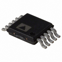
ADP1621ARMZ-R7 Analog Devices Inc, ADP1621ARMZ-R7 Datasheet - Page 22

ADP1621ARMZ-R7
Manufacturer Part Number
ADP1621ARMZ-R7
Description
IC CTRLR DC/DC PWM STEPUP 10MSOP
Manufacturer
Analog Devices Inc
Type
Step-Up (Boost)r
Datasheet
1.ADP1621ARMZ-R7.pdf
(32 pages)
Specifications of ADP1621ARMZ-R7
Internal Switch(s)
No
Synchronous Rectifier
Yes
Number Of Outputs
1
Current - Output
1A
Frequency - Switching
100kHz ~ 1.5MHz
Voltage - Input
2.9 ~ 5.5 V
Operating Temperature
-40°C ~ 125°C
Mounting Type
Surface Mount
Package / Case
10-MSOP, Micro10™, 10-uMAX, 10-uSOP
Primary Input Voltage
5.5V
No. Of Outputs
1
Output Current
1A
No. Of Pins
10
Operating Temperature Range
-40°C To +125°C
Msl
MSL 1 - Unlimited
Frequency Max
1.5MHz
Termination Type
SMD
Lead Free Status / RoHS Status
Lead free / RoHS Compliant
For Use With
ADP1621-EVALZ - BOARD EVALUATION FOR ADP1621
Voltage - Output
-
Power - Output
-
Lead Free Status / RoHS Status
Lead free / RoHS Compliant, Lead free / RoHS Compliant
Other names
ADP1621ARMZ-R7
ADP1621ARMZ-R7TR
ADP1621ARMZ-R7TR
ADP1621
EXAMPLES OF APPLICATION CIRCUITS
STANDARD BOOST CONVERTER—
DESIGN EXAMPLE
The example covered here is for the ADP1621 configured as a
standard boost converter, as shown in Figure 33, where lossless
current sensing is employed. The design parameters are V
3.3 V, V
To begin this design, a switching frequency of 600 kHz is chosen
(by setting R
and small output capacitors can be used. The duty cycle is cal-
culated from Equation 1 to be 0.4, given a forward-voltage drop of
0.5 V for the Schottky diode. The feedback resistors are calculated
to be R1 = 35.7 kΩ and R2 = 11.5 kΩ from Equation 4.
Assuming that the inductor ripple is 30% of 1/(1 − D) times
the maximum load current, the inductor size is calculated to be
about 4.4 μH, according to Equation 9. The small, magnetically
shielded 4.7 μH Toko FDV0630-4R7M inductor is selected.
Because ceramic capacitors have very low ESR (a few milliohms),
a 47 μF/6.3 V Murata GRM31CR60J476M ceramic capacitor is
chosen for the input capacitor. The output voltage ripple for a
given C
By choosing an output voltage ripple equal to 1% of the output
voltage, Equation 12 yields that the minimum C
100 μF and the maximum ESR required is 25 mΩ. Other com-
binations of capacitance and ESR are possible by choosing a
much larger C
ceramic capacitor and two 150 μF Sanyo POSCAP™ capacitors
are selected. The low ESR ceramic capacitor helps to suppress
the high frequency overshoot at the output. POSCAP has low
ESR and high capacitance in a relatively small package. Ceramic
capacitors can also be used. Generally, bigger ceramic capacitors
are more expensive.
OUT
OUT
, ESR, and ESL can be found by solving Equation 12.
= 5 V, and a maximum load current of 1 A.
FREQ
OUT
to 32 kΩ, see Figure 30) so that a small inductor
and a larger ESR. In this case, a small 1 μF
120pF
f
C1 = MURATA GRM31CR60J476M
C
L1 = TOKO FDV0630-4R7M
OSC
OUT3
1µF
10V
C3
C2
= 600kHz
= SANYO POSCAP 6TPE150M
0.1µF
10V
R
9.09kΩ
C4
C
1.8nF
COMP
COMP
R
31.6kΩ
1%
Figure 33. Typical Boost Converter Application Circuit
FREQ
OUT
required is
SDSN
COMP
FREQ
ADP1621
AGND
PIN
IN
GND
M1 = VISHAY Si7882DP
D1 = VISHAY SSA33L
=
PGND
GATE
Rev. A | Page 22 of 32
IN
CS
FB
80Ω
R
S
V
M1
IN
L1
4.7µH
The next step is to choose a Schottky diode. The average
and rms diode currents are calculated to be 1.0 A and 1.3 A,
respectively, using Equations 14 and 15. A Vishay SSA33L
Schottky diode meets the current and thermal requirements
and is an excellent choice.
The power MOSFET must be chosen based on threshold voltage
(V
and gate charge. The rms current through the MOSFET is given
by Equation 18 as 1.1 A. The Vishay Si7882DP is a 20 V n-channel
power MOSFET that meets the current and thermal requirements.
It comes in a PowerPAK® package and offers low R
charge. At V
The loop-compensation components are chosen to be R
9.1 kΩ and C
A roll-off capacitor of C2 = 120 pF is also added. The slope-
compensation resistor is set to be R
Lastly, given the chosen components, the peak inductor current
as set by the current limit circuitry is given by Equation 35 as
I
operation, is given by Equation 36 as I
safely above the 1.0 A load current requirement for this design
example. Note that the current limit is a strong function of R
which can vary part to part and with temperature. In addition,
note that R
sense resistor or with the R
and the other parameters in Equations 35 and 36 must be taken
into account if precise current limiting is necessary. Due to the
parasitic resistance of PCB traces, R
on the actual circuit board to achieve the desired current limit.
Keep in mind that R
with a different R
limit to the desired level.
L,PK
= 3.3V
35.7kΩ
11.5kΩ
T
D1
), on resistance (R
= 12 A. Thus, the maximum load current, assuming CCM
1%
1%
R1
R2
CS
GS
COMP
C1
47µF
6.3V
can be implemented with an external current-
= 2.5 V, the on resistance, R
C
1µF
10V
OUT1
= 1.7 nF from Equations 30 and 31, respectively.
DSON
S
DSON
must be less than 1.6 kΩ. Using a MOSFET
or adjusting R
C
10µF
10V
OUT2
), maximum voltage and current ratings,
V
DSON
OUT
1A
C
150µF
6.3V
×2
= 5V
OUT3
of a MOSFET. Variations in R
S
S
CS
= 80 Ω from Equation 34.
might need to be adjusted
LOAD,MAX
can also set the current
DSON
= 8 A, which is
, is 8 mΩ.
DSON
and gate
COMP
CS
=
CS
,


