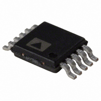
ADP1621ARMZ-R7 Analog Devices Inc, ADP1621ARMZ-R7 Datasheet - Page 5

ADP1621ARMZ-R7
Manufacturer Part Number
ADP1621ARMZ-R7
Description
IC CTRLR DC/DC PWM STEPUP 10MSOP
Manufacturer
Analog Devices Inc
Type
Step-Up (Boost)r
Datasheet
1.ADP1621ARMZ-R7.pdf
(32 pages)
Specifications of ADP1621ARMZ-R7
Internal Switch(s)
No
Synchronous Rectifier
Yes
Number Of Outputs
1
Current - Output
1A
Frequency - Switching
100kHz ~ 1.5MHz
Voltage - Input
2.9 ~ 5.5 V
Operating Temperature
-40°C ~ 125°C
Mounting Type
Surface Mount
Package / Case
10-MSOP, Micro10™, 10-uMAX, 10-uSOP
Primary Input Voltage
5.5V
No. Of Outputs
1
Output Current
1A
No. Of Pins
10
Operating Temperature Range
-40°C To +125°C
Msl
MSL 1 - Unlimited
Frequency Max
1.5MHz
Termination Type
SMD
Lead Free Status / RoHS Status
Lead free / RoHS Compliant
For Use With
ADP1621-EVALZ - BOARD EVALUATION FOR ADP1621
Voltage - Output
-
Power - Output
-
Lead Free Status / RoHS Status
Lead free / RoHS Compliant, Lead free / RoHS Compliant
Other names
ADP1621ARMZ-R7
ADP1621ARMZ-R7TR
ADP1621ARMZ-R7TR
ABSOLUTE MAXIMUM RATINGS
Table 2.
Parameter
IN to GND
FB, COMP, SDSN, FREQ, GATE to GND
CS to GND
PIN to PGND
Supply Current into IN
Supply Current into PIN
Storage Temperature Range
Junction Operating Temperature Range
Junction Storage Temperature Range
Lead Temperature (Soldering, 10 sec)
Package Power Dissipation
1
Stresses above those listed under Absolute Maximum Ratings
may cause permanent damage to the device. This is a stress
rating only; functional operation of the device at these or any
other conditions above those indicated in the operational
section of this specification is not implied. Exposure to absolute
maximum rating conditions for extended periods may affect
device reliability.
In applications where high power dissipation and poor package thermal
resistance are present, the maximum ambient temperature may need to be
derated. Maximum ambient temperature (T
maximum operating junction temperature (T
power dissipation of the device in the application (P
to-ambient thermal resistance of the package in the application (θ
by the following equation: T
A,MAX
1
= T
J,MAX
-- - (θ
A,MAX
JA
J,MAX
x P
1
) is dependent on the
D,MAX
= 150
Rating
−0.3 V to V
−0.3 V to (V
−5 V to +33 V
−0.3 V to V
25 mA
35 mA
−55°C to +150°C
−55°C to +150°C
−55°C to +150°C
300°C
(T
D,MAX
).
J,MAX
o
C), the maximum
), and the junction-
− T
A
)/θ
SHUNT
SHUNT
IN
JA
JA
), is given
+ 0.3 V)
Rev. A | Page 5 of 32
Absolute maximum ratings apply individually only, not in
combination. Unless otherwise specified, all other voltages are
referenced to GND.
THERMAL RESISTANCE
θ
soldered in a circuit board for surface-mount packages.
Table 3. Thermal Resistance
Package Type
10-lead MSOP on a 2-layer PCB
10-lead MSOP on a 4-layer PCB
Junction-to-ambient thermal resistance of the package is based
on modeling and calculation using 2-layer and 4-layer boards,
and natural convection. The junction-to-ambient thermal
resistance is application- and board-layout dependent. In
applications where high maximum power dissipation exists,
attention to thermal dissipation issues in board design is
required.
ESD CAUTION
JA
is specified for the worst-case conditions, that is, a device
θ
200
172
JA
ADP1621
Unit
°C/W
°C/W


