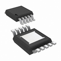
LM25011MY/NOPB National Semiconductor, LM25011MY/NOPB Datasheet - Page 10

LM25011MY/NOPB
Manufacturer Part Number
LM25011MY/NOPB
Description
IC BUCK ADJ 2A 10MSOP
Manufacturer
National Semiconductor
Type
Step-Down (Buck)r
Datasheet
1.LM25011MYNOPB.pdf
(20 pages)
Specifications of LM25011MY/NOPB
Internal Switch(s)
Yes
Synchronous Rectifier
No
Number Of Outputs
1
Voltage - Output
2.51 ~ 40 V
Current - Output
2A
Frequency - Switching
Up to 2MHz
Voltage - Input
6 ~ 42 V
Operating Temperature
-40°C ~ 125°C
Mounting Type
Surface Mount
Package / Case
10-MSOP Exposed Pad, 10-HMSOP, 10-eMSOP
Power - Output
155mW
Primary Input Voltage
42V
No. Of Outputs
1
Output Voltage
40V
Output Current
2A
No. Of Pins
10
Operating Temperature Range
-40°C To +125°C
Msl
MSL 3 - 168 Hours
Filter Terminals
SMD
Rohs Compliant
Yes
Lead Free Status / RoHS Status
Lead free / RoHS Compliant
Other names
LM25011MYTR
Available stocks
Company
Part Number
Manufacturer
Quantity
Price
Company:
Part Number:
LM25011MY/NOPB
Manufacturer:
ATMEL
Quantity:
101
Part Number:
LM25011MY/NOPB
Manufacturer:
TI/德州仪器
Quantity:
20 000
www.national.com
Functional Description
The LM25011 Constant On-time Step-down Switching Reg-
ulator features all the functions needed to implement a low
cost, efficient buck bias power converter capable of supplying
up to 2.0A to the load. This high voltage regulator contains an
N-Channel buck switch, is easy to implement, and is available
in a 10-pin MSOP power enhanced package. The regulator’s
operation is based on a constant on-time control principle with
the on-time inversely proportional to the input voltage. This
feature results in the operating frequency remaining relatively
constant with load and input voltage variations. The constant
on-time feedback control principle requires no loop compen-
sation resulting in very fast load transient response. The
adjustable valley current limit detection results in a smooth
transition from constant voltage to constant current when cur-
rent limit is reached. To aid in controlling excessive switch
current due to a possible saturating inductor the on-time is
reduced by
Good output (PGD pin) indicates when the output voltage is
within 5% of the expected regulation voltage.
The LM25011 can be implemented to efficiently step-down
higher voltages in non-isolated applications. Additional fea-
tures include: Low output ripple, VIN under-voltage lock-out,
adjustable soft-start timing, thermal shutdown, gate drive pre-
≊
40% when current limit is detected. The Power
FIGURE 1. Startup Sequence
10
charge, gate drive under-voltage lock-out, and maximum duty
cycle limit.
Control Circuit Overview
The LM25011 buck regulator employs a control principle
based on a comparator and a one-shot on-timer, with the out-
put voltage feedback (FB) compared to an internal reference
(2.51V). If the FB voltage is below the reference the internal
buck switch is switched on for the one-shot timer period,
which is a function of the input voltage and the programming
resistor (R
the FB voltage falls below the reference, but never less than
the minimum off-time forced by the off-time one-shot timer.
When the FB pin voltage falls below the reference and the off-
time one-shot period expires, the buck switch is then turned
on for another on-time one-shot period.
When in regulation, the LM25011 operates in continuous con-
duction mode at heavy load currents and discontinuous con-
duction mode at light load currents. In continuous conduction
mode the inductor’s current is always greater than zero, and
the operating frequency remains relatively constant with load
and line variations. The minimum load current for continuous
conduction mode is one-half the inductor’s ripple current am-
T
). Following the on-time the switch remains off until
30094618


