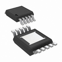
LM25011MY/NOPB National Semiconductor, LM25011MY/NOPB Datasheet - Page 15

LM25011MY/NOPB
Manufacturer Part Number
LM25011MY/NOPB
Description
IC BUCK ADJ 2A 10MSOP
Manufacturer
National Semiconductor
Type
Step-Down (Buck)r
Datasheet
1.LM25011MYNOPB.pdf
(20 pages)
Specifications of LM25011MY/NOPB
Internal Switch(s)
Yes
Synchronous Rectifier
No
Number Of Outputs
1
Voltage - Output
2.51 ~ 40 V
Current - Output
2A
Frequency - Switching
Up to 2MHz
Voltage - Input
6 ~ 42 V
Operating Temperature
-40°C ~ 125°C
Mounting Type
Surface Mount
Package / Case
10-MSOP Exposed Pad, 10-HMSOP, 10-eMSOP
Power - Output
155mW
Primary Input Voltage
42V
No. Of Outputs
1
Output Voltage
40V
Output Current
2A
No. Of Pins
10
Operating Temperature Range
-40°C To +125°C
Msl
MSL 3 - 168 Hours
Filter Terminals
SMD
Rohs Compliant
Yes
Lead Free Status / RoHS Status
Lead free / RoHS Compliant
Other names
LM25011MYTR
Available stocks
Company
Part Number
Manufacturer
Quantity
Price
Company:
Part Number:
LM25011MY/NOPB
Manufacturer:
ATMEL
Quantity:
101
Part Number:
LM25011MY/NOPB
Manufacturer:
TI/德州仪器
Quantity:
20 000
FIGURE 7. Frequency vs V
FIGURE 6. Efficiency (Circuit of
IN
(Circuit of
Figure
Figure
30094603
30094636
FIGURE 5. Example Circuit
5)
5)
15
OUTPUT RIPPLE CONTROL (LM25011A)
The LM25011A most likely will require more ripple voltage
than is generated across the RS resistor. Additional ripple can
be supplied to the FB pin, in phase with the switching wave-
form at the SW pin, for proper operation. The required ripple
can be supplied from ripple generated at V
feedback resistors, as described in Option A below. Options
B and C provide for lower output ripple with one or two addi-
tional components.
The amount of additional ripple voltage needed at the FB pin
is typically in the range of 30-150mV. Higher switching fre-
quencies or higher inductor values (less ripple current) re-
quire more ripple voltage injected on FB. Insufficient ripple
voltage will result in frequency jitter. For a particular applica-
tion, add only as much ripple as needed to stabilize the
switching frequency over the required input voltage.
Option A) Lowest Cost Configuration: In this configuration
R1 is installed in series with the output capacitor (C
shown in Figure 8. The inductor’s ripple current passes
through R1, generating a ripple voltage at V
value for R1 is:
where ΔI is the minimum ripple current amplitude, which oc-
curs at minimum Vin.
30094634
OUT
OUT
. The minimum
, through the
www.national.com
OUT
) as


