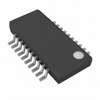
MAX1962EEP+ Maxim Integrated Products, MAX1962EEP+ Datasheet - Page 19

MAX1962EEP+
Manufacturer Part Number
MAX1962EEP+
Description
IC DC-DC CTRL STP DWN 20-QSOP
Manufacturer
Maxim Integrated Products
Type
Step-Down (Buck)r
Datasheet
1.MAX1960EEP.pdf
(29 pages)
Specifications of MAX1962EEP+
Internal Switch(s)
No
Synchronous Rectifier
No
Number Of Outputs
1
Voltage - Output
0.8 ~ 4.95 V
Current - Output
20A
Frequency - Switching
500kHz, 1MHz
Voltage - Input
2.35 ~ 5.5 V
Operating Temperature
-40°C ~ 85°C
Mounting Type
Surface Mount
Package / Case
20-QSOP
Power - Output
727mW, 9.1mW
Lead Free Status / RoHS Status
Lead free / RoHS Compliant
Figure 7. Open-Loop Transfer Model
At high switching rates, dynamic characteristics (para-
meters 1, 2, 5, and 6) that predict switching losses may
have more impact on efficiency than R
dicts DC losses. Q
with charging the gate, and best performance is
achieved with a low total gate charge. Q
predict the current needed to drive the gate at the
selected operating frequency. This is very important
because the output current from the charge pump is
finite (50mA, max) and is used to drive the gates of the
MOSFETs as well as provide bias for the IC. R
important as well, as it is used for current sensing in the
MAX1960/MAX1961. R
pation during the on-time of the MOSFET.
Choose Q
Step-Down Controllers with Voltage Margining
(4) Gate threshold voltage (V
(5) Turn-on/turn-off times
(6) Turn-on/turn-off delays
FEEDBACK DIVIDER
G
V
1
to be as low as possible. Ensure that:
2.35V to 5.5V, 0.5% Accurate, 1MHz PWM
Q
______________________________________________________________________________________
G
R2
R1
G
1
includes all capacitance associated
+
DS(ON)
Q
G
2
≤
50
0.8V
also causes power dissi-
f
mA
S
TH(MIN)
ERROR AMPLIFIER
DS(ON)
Gm
)
G
, which pre-
also helps
DS(ON)
R3
C9
is
Choose R
the desired current-limit threshold voltage (see the
Setting the Current Limit section).
Fast-switching transitions can cause ringing due to res-
onating circuit parasitic inductance and capacitance at
the switching nodes. This high-frequency ringing
occurs at LX rising and falling transitions, and may
introduce current-sensing errors and generate EMI. To
dampen this ringing, a series RC snubber circuit can
be added across each MOSFET switch (Figure 8).
Typical values for the snubber components are C
= 4700pF and R
for snubber components will depend on circuit para-
sitics. Below is the procedure for selecting the compo-
nent values of the series RC snubber circuit:
1) Connect a scope probe to measure V
2) Find the capacitor value (connected from LX to
3) The circuit parasitic capacitance, C
MODULATOR
V
and observe the ringing frequency, f
GND) that reduces the ringing frequency by half.
equal to 1/3 of the value of the added capacitance
above.
IN
/V
RAMP
DS(ON)
SNUB
to provide the desired I
= 1Ω, however, the ideal values
MOSFET RC Snubber Circuit
OUTPUT FILTER
R
R
S
C
ESR
L1
OUT
V
2
R
PAR
LOAD
R
.
LOAD(MAX)
, at LX is then
LX
to GND,
SNUB
19
at


