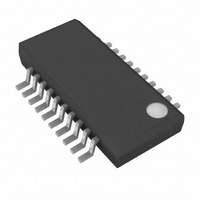
MAX1962EEP+ Maxim Integrated Products, MAX1962EEP+ Datasheet - Page 20

MAX1962EEP+
Manufacturer Part Number
MAX1962EEP+
Description
IC DC-DC CTRL STP DWN 20-QSOP
Manufacturer
Maxim Integrated Products
Type
Step-Down (Buck)r
Datasheet
1.MAX1960EEP.pdf
(29 pages)
Specifications of MAX1962EEP+
Internal Switch(s)
No
Synchronous Rectifier
No
Number Of Outputs
1
Voltage - Output
0.8 ~ 4.95 V
Current - Output
20A
Frequency - Switching
500kHz, 1MHz
Voltage - Input
2.35 ~ 5.5 V
Operating Temperature
-40°C ~ 85°C
Mounting Type
Surface Mount
Package / Case
20-QSOP
Power - Output
727mW, 9.1mW
Lead Free Status / RoHS Status
Lead free / RoHS Compliant
Worst-case power dissipation occurs at duty factor
extremes. For the high-side MOSFET, the worst-case
power dissipation due to resistance occurs at minimum
input voltage (V
The following formula calculates switching losses for
the high-side MOSFET, but is only an approximation
and not a substitute for evaluation:
2.35V to 5.5V, 0.5% Accurate, 1MHz PWM
Step-Down Controllers with Voltage Margining
Figure 8. RC Snubber Circuit
20
(
I
L PEAK
4) The circuit parasitic inductance, L
5) The resistor for critical dampening, R
6) The capacitor, C
7) The snubber circuit power loss is dissipated in the
(
PD
______________________________________________________________________________________
where V
switching frequency. Choose R
that exceeds the calculated power dissipation.
by:
f
or down to tailor the desired damping and the
peak voltage excursion.
times the value of the C
resistor, P
R
(
N RESISTIVE
x L
)
1
MAX1960
×
PAR
P
t
RSNUB
FALL
IN
L
. The resistor value can be adjusted up
RSNUB
PGND
IN(MIN)
PAR
DH
DL
is the input voltage, and f
LX
+
)
P
I
=
D N SWITCHING
L VALLEY
=
=
(
(
, and can be calculated as:
(
):
SNUB
V
2
1
C
IN MIN
V
π
OUT
SNUB
(
MOSFET Power Dissipation
×
INPUT
, should be at least 2 to 4
)
PAR
f
N1
N2
R
)
×
)
1
2
×
×
t
to be effective.
RISE
×
)
(
I
V
LOAD
=
IN
C
SNUB
R
C
R
C
)
PAR
SNUB
SNUB
)
SNUB
SNUB
PAR
2
×
2
×
V
, is calculated
IN MAX
SNUB
×
power rating
f
S
(
L1
2
R
DS ON
S
)
= 2π x
is the
(
×
)
f
S
where V
age, t
MOSFET, I
peak and valley inductor current, and f
switching frequency:
where LIR is the peak-to-peak inductor ripple current
divided by the load current.
The total power dissipation in the high-side MOSFET is
the sum of these two power losses:
For the low-side MOSFET, the worst-case power dissi-
pation occurs at maximum input voltage:
A properly designed PC board layout is important in
any switching DC-DC converter circuit. If possible,
mount the MOSFETs, inductor, input/output capacitors,
and current-sense resistor on the top side. Connect the
ground for these devices close together on a power-
ground trace. Make all other ground connections to a
separate analog ground plane. Connect the analog
ground plane to power ground at a single point.
To help dissipate heat, place high-power components
(MOSFETs, inductor, and current-sense resistor) on a
large PC board area. Keep high-current traces short and
wide to reduce the resistance in these traces. Also make
the gate drive connections (DH and DL) short and wide,
measuring 10 to 20 squares (50mils to 100mils wide if the
MOSFET is 1in from the controller IC).
For the MAX1960/MAX1961, connect LX and PGND to
the low-side MOSFET using Kelvin sense connections.
For the MAX1962, connect CS and OUT to the current-
sense resistor using Kelvin sense connections.
Place the REF capacitor, the BST diode and capacitor,
and the charge-pump components as close as possible
to the IC. If the IC is far from the input capacitors, bypass
V
close to the V
For an example PC board layout, see the MAX1960
evaluation kit.
I
P
L(PEAK)
CC
D N RESISTIVE
(
2
to GND with a 0.1µF or greater ceramic capacitor
P
FALL
D(N1)
IN(MAX)
= I
L(PEAK)
and t
OUT(MAX)
= P
CC
I
)
OUT(MAX)
Applications Information
D(N1RESISTIVE)
is the maximum value of the input volt-
=
pin.
RISE
⎛
⎜
⎝
1
PC Board Layout Guidelines
and I
-
× (1 + 0.5 × LIR) and I
are the fall and rise time of the
V
IN MAX
V
× (1 - 0.5 × LIR)
OUT
(
L(VALLEY)
)
+ P
⎞
⎟ ×
⎠
D(N1SWITCHING)
I
LOAD
are the maximum
S
2
is the PWM
L(VALLEY)
×
R
DS ON
(
=
)


