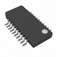
MAX1962EEP+ Maxim Integrated Products, MAX1962EEP+ Datasheet - Page 2

MAX1962EEP+
Manufacturer Part Number
MAX1962EEP+
Description
IC DC-DC CTRL STP DWN 20-QSOP
Manufacturer
Maxim Integrated Products
Type
Step-Down (Buck)r
Datasheet
1.MAX1960EEP.pdf
(29 pages)
Specifications of MAX1962EEP+
Internal Switch(s)
No
Synchronous Rectifier
No
Number Of Outputs
1
Voltage - Output
0.8 ~ 4.95 V
Current - Output
20A
Frequency - Switching
500kHz, 1MHz
Voltage - Input
2.35 ~ 5.5 V
Operating Temperature
-40°C ~ 85°C
Mounting Type
Surface Mount
Package / Case
20-QSOP
Power - Output
727mW, 9.1mW
Lead Free Status / RoHS Status
Lead free / RoHS Compliant
ABSOLUTE MAXIMUM RATINGS
V
ILIM, COMP, REF, FB, CLKOUT,
C+ to GND.............-0.3V to higher of V
V
DL to PGND ................................................-0.3V to V
BST to GND ............................................................-0.3V to +12V
DH to LX ...................................................................-0.3V to +6V
LX to BST..................................................................-6V to +0.3V
PGND to GND, or V
2.35V to 5.5V, 0.5% Accurate, 1MHz PWM
Step-Down Controllers with Voltage Margining
ELECTRICAL CHARACTERISTICS
(V
Stresses beyond those listed under “Absolute Maximum Ratings” may cause permanent damage to the device. These are stress ratings only, and functional
operation of the device at these or any other conditions beyond those indicated in the operational sections of the specifications is not implied. Exposure to
absolute maximum rating conditions for extended periods may affect device reliability.
2
V
V
V
Output Voltage
DC Output Accuracy
Positive Voltage-Margining Shift
Negative Voltage-Margining Shift
Load Regulation Error
Line Regulation Error
FB Input Bias Current
Feedback Transconductance
COMP Discharge Resistance
DC-DC Soft-Start Time
Switching Frequency
SYNC Frequency Range
Maximum Duty Cycle
Maximum Duty Cycle
Quiescent Supply Current
Shutdown Supply Current
CC
DD
OUT to GND ..........................................................-0.3V to +6V
C- to GND ..............................................-0.3V to V
VCC
CC
CC
DD
, CTL_, CS, FSET/SYNC, SEL, EN,
, AV
_______________________________________________________________________________________
Input Voltage Range
Input Voltage UVLO
Input Voltage UVLO
= 3.3V, Circuits of Figures 9–12, T
DD
to GND ..............-0.3V to higher of V
PARAMETER
DD
to AV
DD
............................-0.3V to +0.3V
VCC
A
+ 1V or V
= 0°C to +85°C. Typical values are at T
Rising or falling, hysteresis = 33mV (typ)
Rising or falling, hysteresis = 44mV (typ)
MAX1960/MAX1962 (measured at FB)
MAX1961/
MAX1962 (FB = V
measured at output
MAX1960/MAX1961
MAX1960/MAX1961
0V to full load
V
In shutdown
FSET/SYNC = GND
FSET/SYNC = V
f = 1MHz
f = 500kHz
VCC
VCC
AVDD
= 2.7V to 5.5V
- 0.3V or 6V
VDD
VDD
+ 0.3V
+ 0.3V
+ 0.3V
CC
CONDITIONS
DD
),
SEL = GND
SEL = REF
SEL not connected
SEL = V
Continuous Power Dissipation (T
Operating Temperature Range (Extended).........-40°C to +85°C
Junction Temperature ......................................................+150°C
Storage Temperature Range .............................-65°C to +150°C
Lead Temperature (soldering, 10s) .................................+300°C
20-Pin QSOP (derate up to +70°C)..............................727mW
20-Pin QSOP (derate above +70°C) ........................9.1mW/°C
DD
A
= +25°C, unless otherwise noted.)
0.796
1.492
1.791
2.487
3.272
+3.8
MIN
2.35
1.95
-3.8
-0.2
450
880
450
3.9
0.8
80
90
1
A
= +70°C)
0.800
1.500
1.800
2.500
3.300
1280
1000
TYP
0.08
500
0.1
+4
10
83
92
11
-4
2
0.804
1.508
1.809
2.514
3.336
MAX
1120
1200
+4.2
+0.2
4.45
-4.2
100
550
5.5
2.3
15
15
3
UNITS
cycles
kHz
kHz
mS
mA
µA
µA
%
%
%
%
%
%
Ω
V
V
V
V
V


