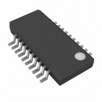
MAX1962EEP+ Maxim Integrated Products, MAX1962EEP+ Datasheet - Page 9

MAX1962EEP+
Manufacturer Part Number
MAX1962EEP+
Description
IC DC-DC CTRL STP DWN 20-QSOP
Manufacturer
Maxim Integrated Products
Type
Step-Down (Buck)r
Datasheet
1.MAX1960EEP.pdf
(29 pages)
Specifications of MAX1962EEP+
Internal Switch(s)
No
Synchronous Rectifier
No
Number Of Outputs
1
Voltage - Output
0.8 ~ 4.95 V
Current - Output
20A
Frequency - Switching
500kHz, 1MHz
Voltage - Input
2.35 ~ 5.5 V
Operating Temperature
-40°C ~ 85°C
Mounting Type
Surface Mount
Package / Case
20-QSOP
Power - Output
727mW, 9.1mW
Lead Free Status / RoHS Status
Lead free / RoHS Compliant
MAX1960 MAX1961 MAX1962
Step-Down Controllers with Voltage Margining
10
11
12
13
14
—
—
—
—
1
2
3
4
5
6
7
8
9
PIN
10
11
12
13
14
—
—
—
—
1
2
3
4
8
5
6
7
9
2.35V to 5.5V, 0.5% Accurate, 1MHz PWM
_______________________________________________________________________________________
10
11
12
13
14
—
—
—
—
1
2
3
4
5
6
7
8
9
FSET/SYNC
CLKOUT
NAME
COMP
PGND
AV
CTL1
CTL2
GND
N.C.
OUT
ILIM
V
SEL
REF
EN
CS
DL
FB
DD
DD
Clock Output. Connect to FSET/SYNC of a second converter to operate 180° out-of-
phase. CLKOUT swings from V
Operating Frequency and Synchronization section).
Frequency Set and Synchronization. Connect to GND for 500kHz operation,
connect to V
(between 450kHz and 1200kHz).
Current Limit. Connect a resistor from ILIM to GND to set the current-sense
threshold voltage. Connect ILIM to V
E nab l e. D r i ve hi g h for nor m al op er ati on. D r i ve l ow or connect to GN D for shutd ow n m od e.
Preset Output Voltage Select. Allows the output to be set to one of four preset
voltages (1.5V, 1.8V, 2.5V, and 3.3V). For the MAX1962, FB must be connected to
V
No Connection. Not internally connected.
Output. Connect to the output. Used to sense the output voltage for internal
feedback and current sense.
Control Pins. Controls voltage margining and shutdown. Connect both CTL1 and
CTL2 high for normal operation. Connect both CTL1 and CTL2 low for shutdown.
Connect CTL1 high and CTL2 low for +4% voltage margining. Connect CTL1 low
and CTL2 high for -4% voltage margining. If voltage margining is not to be used,
connect CTL1 and CTL2 together and use to enable/shutdown the device.
C ur r ent- S ense Inp ut. C onnect to the j uncti on of the cur r ent- sense r esi stor and the
i nd uctor . The M AX 1962 cur r ent- sense thr eshol d i s 50m V m easur ed fr om C S to O U T.
Filtered Supply from V
in shutdown. Do not apply an external load to AV
Feed b ack Inp ut. The feed b ack thr eshol d i s 0.8V . C onnect to the center of a r esi sti ve
vol tag e- d i vi d er fr om the outp ut to GN D to set the outp ut vol tag e to 0.8V or g r eater . On
the M AX 1962, connect FB to V
Compensation Pin. COMP is forced to GND in shutdown, UVLO, or thermal fault.
Reference Output. V
Analog Ground. Connect to the PC board analog ground plane. Connect the PC
board analog ground plane and power ground planes with a single connection.
C har g e- P um p O utp ut. P r ovi d es r eg ul ated 5V to p ow er the IC and g ate d r i ver s.
Byp ass w i th a 4.7µF cer am i c cap aci tor for op er ati ng fr eq uenci es b etw een 450kH z
and 950kH z. Byp ass w i th a 2.2µF cer am i c cap aci tor for 1M H z op er ati on. V
i nter nal l y for ced to V
Low-Side MOSFET Synchronous Rectifier Gate-Driver Output. DL is high in
shutdown.
Power Ground. Connect to the PC board power ground plane.
DD
if SEL is to be used (see the Setting the Output Voltage section).
CC
for 1MHz operation, or drive with clock signal to synchronize
CC
REF
DD
i n shutd ow n. D o not ap p l y an exter nal l oad to V
= 1.28V. Bypass with a 0.22µF capacitor to GND.
. Connect a 1µF bypass capacitor. AV
DD
CC
to sel ect p r eset outp ut vol tag es ( see S E L) .
to GND. CLKOUT is low in shutdown (see the
FUNCTION
DD
to select the default threshold of 75mV.
DD
.
Pin Description
DD
is forced to V
DD
.
DD
i s
CC
9


