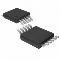
LTC1871EMS-7 Linear Technology, LTC1871EMS-7 Datasheet - Page 23

LTC1871EMS-7
Manufacturer Part Number
LTC1871EMS-7
Description
IC MULTI CONFIG SYNC ADJ 10MSOP
Manufacturer
Linear Technology
Type
Step-Up (Boost), Flyback, Sepicr
Datasheet
1.LTC1871EMS-7.pdf
(32 pages)
Specifications of LTC1871EMS-7
Internal Switch(s)
No
Synchronous Rectifier
No
Number Of Outputs
1
Voltage - Output
1.23 ~ 36 V
Current - Output
50mA
Frequency - Switching
50kHz ~ 1MHz
Voltage - Input
6 ~ 36 V
Operating Temperature
-40°C ~ 85°C
Mounting Type
Surface Mount
Package / Case
10-MSOP, Micro10™, 10-uMAX, 10-uSOP
Lead Free Status / RoHS Status
Contains lead / RoHS non-compliant
Power - Output
-
Available stocks
Company
Part Number
Manufacturer
Quantity
Price
Company:
Part Number:
LTC1871EMS-7
Manufacturer:
LT
Quantity:
10 000
APPLICATIONS INFORMATION
7. Minimize the capacitance between the SENSE pin trace
and any high frequency switching nodes. The LTC1871-7
contains an internal leading edge blanking time of ap-
proximately 180ns, which should be adequate for most
applications.
R2
OUTPUT SENSING
SIGNAL GROUND
VIAS TO GROUND
PLANE
PSEUDO-KELVIN
R
R
TRUE REMOTE
C
T
R1
CONNECTION
C
C
R3
PIN 1
LTC1871-7
R4
BOLD LINES INDICATE HIGH CURRENT PATHS
R2
C
OUT
R1
R
C
C
C
T
VCC
Figure 18. LTC1871-7 Boost Converter Suggested Layout
Figure 19. LTC1871-7 Boost Converter Layout Diagram
R
R3
C
1
2
3
4
5
C
GROUND CONNECTION
C
OUT
RUN
I
LTC1871-7
FB
FREQ
MODE/
SYNC
IN
TH
R4
PSEUDO-KELVIN
INTV
SENSE
GATE
GND
R
V
S
CC
IN
10
9
8
7
6
8. For optimum load regulation and true remote sens-
ing, the top of the output resistor divider should connect
independently to the top of the output capacitor (Kelvin
connection), staying away from any high dV/dt traces.
Place the divider resistors near the LTC1871-7 in order
to keep the high impedance FB node short.
JUMPER
J1
J1
C
VCC
+
+
C
C
IN
OUT
M1
L1
D1
L1
M1
R
SWITCH
S
NODE
18717 F19
D1
V
GND
V
IN
OUT
1871 F18
V
V
IN
LTC1871-7
OUT
SWITCH NODE IS ALSO
THE HEAT SPREADER
FOR L1, M1, D1
23
18717fc


