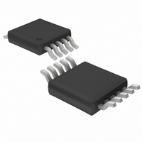
LTC1871EMS-7 Linear Technology, LTC1871EMS-7 Datasheet - Page 24

LTC1871EMS-7
Manufacturer Part Number
LTC1871EMS-7
Description
IC MULTI CONFIG SYNC ADJ 10MSOP
Manufacturer
Linear Technology
Type
Step-Up (Boost), Flyback, Sepicr
Datasheet
1.LTC1871EMS-7.pdf
(32 pages)
Specifications of LTC1871EMS-7
Internal Switch(s)
No
Synchronous Rectifier
No
Number Of Outputs
1
Voltage - Output
1.23 ~ 36 V
Current - Output
50mA
Frequency - Switching
50kHz ~ 1MHz
Voltage - Input
6 ~ 36 V
Operating Temperature
-40°C ~ 85°C
Mounting Type
Surface Mount
Package / Case
10-MSOP, Micro10™, 10-uMAX, 10-uSOP
Lead Free Status / RoHS Status
Contains lead / RoHS non-compliant
Power - Output
-
Available stocks
Company
Part Number
Manufacturer
Quantity
Price
Company:
Part Number:
LTC1871EMS-7
Manufacturer:
LT
Quantity:
10 000
LTC1871-7
APPLICATIONS INFORMATION
9. For applications with multiple switching power convert-
ers connected to the same input supply, make sure that
the input fi lter capacitor for the LTC1871-7 is not shared
with other converters. AC input current from another
converter could cause substantial input voltage ripple, and
this could interfere with the operation of the LTC1871-7.
A few inches of PC trace or wire (L ≈ 100nH) between the
C
suffi cient to prevent current sharing problems.
SEPIC Converter Applications
The LTC1871-7 is also well suited to SEPIC (single-ended
primary inductance converter) converter applications. The
SEPIC converter shown in Figure 20 uses two inductors.
The advantage of the SEPIC converter is the input voltage
may be higher or lower than the output voltage, and the
output is short-circuit protected.
The fi rst inductor, L1, together with the main switch,
resembles a boost converter. The second inductor, L2,
together with the output diode D1, resembles a fl yback or
buck-boost converter. The two inductors L1 and L2 can be
independent but can also be wound on the same core since
identical voltages are applied to L1 and L2 throughout the
switching cycle. By making L1 = L2 and winding them on
the same core the input ripple is reduced along with cost
24
IN
of the LTC1871-7 and the actual source V
V
V
V
IN
IN
IN
+
+
+
Figure 20. SEPIC Topolgy and Current Flow
20b. Current Flow During Switch On-Time
20c. Current Flow During Switch Off-Time
•
•
•
L1
SW
20a. SEPIC Topology
+
+
+
V
V
C1
IN
IN
L2
•
•
•
D1
D1
C
OUT
+
+
+
V
V
V
OUT
OUT
OUT
18717 F20
IN
should be
R
R
R
L
L
L
and size. All of the SEPIC applications information that
follows assumes L1 = L2 = L.
SEPIC Converter: Duty Cycle Considerations
For a SEPIC converter operating in a continuous conduction
mode (CCM), the duty cycle of the main switch is:
where V
ers where the input voltage is close to the output voltage
the duty cycle is near 50%.
D =
Figure 21. SEPIC Converter Switching Waveforms
D
V
IN
is the forward voltage of the diode. For convert-
V
21c. DC Coupling Capacitor Current
(AC)
V
OUT
I
I
I
I
+ V
D1
L1
L2
C1
O
21b. Output Inductor Current
+ V
21a. Input Inductor Current
21e. Output Ripple Voltage
O
SW
ON
+ V
D
21d. Diode Current
D
ΔV
OFF
SW
ESR
RINGING DUE TO
TOTAL INDUCTANCE
(BOARD + CAP)
ΔV
COUT
18717 F21
I
I
I
I
I
IN
O
IN
O
O
18717fc


