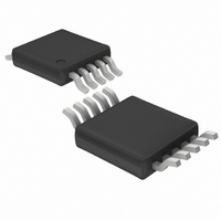
LTC1871EMS-7 Linear Technology, LTC1871EMS-7 Datasheet - Page 7

LTC1871EMS-7
Manufacturer Part Number
LTC1871EMS-7
Description
IC MULTI CONFIG SYNC ADJ 10MSOP
Manufacturer
Linear Technology
Type
Step-Up (Boost), Flyback, Sepicr
Datasheet
1.LTC1871EMS-7.pdf
(32 pages)
Specifications of LTC1871EMS-7
Internal Switch(s)
No
Synchronous Rectifier
No
Number Of Outputs
1
Voltage - Output
1.23 ~ 36 V
Current - Output
50mA
Frequency - Switching
50kHz ~ 1MHz
Voltage - Input
6 ~ 36 V
Operating Temperature
-40°C ~ 85°C
Mounting Type
Surface Mount
Package / Case
10-MSOP, Micro10™, 10-uMAX, 10-uSOP
Lead Free Status / RoHS Status
Contains lead / RoHS non-compliant
Power - Output
-
Available stocks
Company
Part Number
Manufacturer
Quantity
Price
Company:
Part Number:
LTC1871EMS-7
Manufacturer:
LT
Quantity:
10 000
PIN FUNCTIONS
MODE/SYNC (Pin 5): This input controls the operating
mode of the converter and allows for synchronizing the
operating frequency to an external clock. If the MODE/
SYNC pin is connected to ground, Burst Mode operation
is enabled. If the MODE/SYNC pin is connected to INTV
or if an external logic-level synchronization signal is ap-
plied to this input, Burst Mode operation is disabled and
the IC operates in a continuous mode.
GND (Pin 6): Ground Pin.
GATE (Pin 7): Gate Driver Output.
INTV
gate driver and control circuits are powered from this
voltage. Decouple this pin locally to the IC ground with
BLOCK DIAGRAM
CC
(Pin 8): The Internal 7V Regulator Output. The
1.230V
MODE/SYNC
4.6V DOWN
INTV
FREQ
I
FB
5.6V UP
4
5
3
TH
2
8
1.230V
CC
85mV
+
0.6V
–
+
–
+
7V
–
+
g
m
V-TO-I
LDO
OV
EA
UV
0.30V
1.230V
I
OSC
TO
START-UP
CONTROL
50k
+
–
COMPENSATION
COMPARATOR
CC
SLOPE
SLOPE
V-TO-I
BURST
BIAS
OSC
V
,
IN
a minimum of 4.7μF low ESR tantalum or ceramic ca-
pacitor. This 7V regulator has an undervoltage lockout
circuit with 5.6V and 4.6V rising and falling thresholds,
respectively.
V
to ground.
SENSE (Pin 10): The Current Sense Input for the Control
Loop. Connect this pin to a resistor in the source of the
power MOSFET. Alternatively, the SENSE pin may be con-
nected to the drain of the power MOSFET, in applications
where the maximum V
edge blanking is provided for both sensing methods.
IN
(Pin 9): Main Supply Pin. Must be closely decoupled
1.230V
I
V
LOOP
REF
START-UP
BIAS AND
CONTROL
PWM LATCH
R
S
COMPARATOR
CURRENT
Q
LOGIC
DS
C1
is less than 36V. Internal leading
+
–
C2
INTV
+
–
GND
R
LOOP
CC
SENSE
18717 BD
LTC1871-7
1.248V
GATE
RUN
GND
V
10
1
9
7
6
IN
18717fc
7


