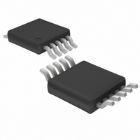
LTC1871EMS-1#PBF Linear Technology, LTC1871EMS-1#PBF Datasheet - Page 19

LTC1871EMS-1#PBF
Manufacturer Part Number
LTC1871EMS-1#PBF
Description
IC CONTRLR CURRENT MODE 10-MSOP
Manufacturer
Linear Technology
Type
Step-Up (Boost), Flyback, Sepicr
Datasheet
1.LTC1871EMS-1PBF.pdf
(36 pages)
Specifications of LTC1871EMS-1#PBF
Internal Switch(s)
No
Synchronous Rectifier
No
Number Of Outputs
1
Voltage - Output
1.23 ~ 72 V
Current - Output
50mA
Frequency - Switching
50kHz ~ 1MHz
Voltage - Input
2.5 ~ 36 V
Operating Temperature
-40°C ~ 85°C
Mounting Type
Surface Mount
Package / Case
10-MSOP, Micro10™, 10-uMAX, 10-uSOP
Lead Free Status / RoHS Status
Lead free / RoHS Compliant
Power - Output
-
Available stocks
Company
Part Number
Manufacturer
Quantity
Price
APPLICATIONS INFORMATION
Burst Mode operations begins, since it is the peak current
that is being clamped.
The output voltage ripple can increase during Burst Mode
operation if ΔI
occur if the input voltage is very low or if a very large
inductor is chosen. At high duty cycles, a skipped cycle
causes the inductor current to quickly decay to zero.
However, because ΔI
for the current to ramp back up to I
ing this inductor charging interval, the output capacitor
must supply the load current and a signifi cant droop in
the output voltage can occur. Generally, it is a good idea
to choose a value of inductor ΔI
of I
of the output capacitor or disable Burst Mode operation
using the MODE/SYNC pin.
Burst Mode operation can be defeated by connecting the
MODE/SYNC pin to a high logic-level voltage (either with
a control input or by connecting this pin to INTV
this mode, the burst clamp is removed, and the chip can
operate at constant frequency from continuous conduction
mode (CCM) at full load, down into deep discontinuous
conduction mode (DCM) at light load. Prior to skipping
pulses at very light load (i.e., < 5% of full load), the
controller will operate with a minimum switch on-time
in DCM. Pulse skipping prevents a loss of control of
the output at very light loads and reduces output volt-
age ripple.
Effi ciency Considerations: How Much Does V
Sensing Help?
The effi ciency of a switching regulator is equal to the
output power divided by the input power (×100%).
Percent effi ciency can be expressed as:
where L1, L2, etc. are the individual loss components
as a percentage of the input power. It is often useful to
analyze individual losses to determine what is limiting
the effi ciency and which change would produce the most
improvement. Although all dissipative elements in the
circuit produce losses, four main sources usually account
for the majority of the losses in LTC1871-1 applica-
tion circuits:
% Effi ciency = 100% – (L1 + L2 + L3 + …),
IN(MAX)
. The alternative is to either increase the value
L
is substantially less than I
L
is small, it takes multiple cycles
L
between 25% and 40%
BURST(PEAK)
BURST
DS
. This can
CC
. Dur-
). In
1. The supply current into V
2. Power MOSFET switching and conduction losses. The
sum of the DC supply current I
Characteristics) and the MOSFET driver and control
currents. The DC supply current into the V
cally about 550μA and represents a small power loss
(much less than 1%) that increases with V
current results from switching the gate capacitance
of the power MOSFET; this current is typically much
larger than the DC current. Each time the MOSFET is
switched on and then off, a packet of gate charge Q
is transferred from INTV
dQ/dt is a current that must be supplied to the INTV
capacitor through the V
the IC is operating in CCM:
technique of using the voltage drop across the power
MOSFET to close the current feedback loop was chosen
because of the increased effi ciency that results from
not having a sense resistor. The losses in the power
MOSFET are equal to:
The I
discrete sense resistor can be calculated almost by
inspection.
To understand the magnitude of the improvement with
this V
5V output power supply shown in Figure 1. The maxi-
mum load current is 7A (10A peak) and the duty cycle
is 39%. Assuming a ripple current of 40%, the peak
inductor current is 13.8A and the average is 11.5A.
With a maximum sense voltage of about 140mV, the
sense resistor value would be 10mΩ, and the power
I
P
P
Q(TOT)
R(SENSE)
IC
2
P
DS
R power savings that result from not having a
= V
FET
sensing technique, consider the 3.3V input,
IN
≈ I
=
+k • V
• (I
=
Q
1– D
I
= f • Q
O(MAX)
Q
1– D
O
I
+ f • Q
O(MAX)
1.85
MAX
MAX
G
•
(
G
IN
2
1– D
)
I
O(MAX)
CC
• R
2
pin by an external supply. If
IN
• R
DS(ON)
MAX
to ground. The resulting
. The V
SENSE
Q
(given in the Electrical
)
LTC1871-1
• C
• D
• D
RSS
IN
MAX
MAX
current is the
• f
IN
IN
•
. The driver
pin is typi-
T
19
18711fb
CC
G


