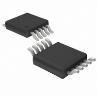
LTC1871EMS-1#PBF Linear Technology, LTC1871EMS-1#PBF Datasheet - Page 23

LTC1871EMS-1#PBF
Manufacturer Part Number
LTC1871EMS-1#PBF
Description
IC CONTRLR CURRENT MODE 10-MSOP
Manufacturer
Linear Technology
Type
Step-Up (Boost), Flyback, Sepicr
Datasheet
1.LTC1871EMS-1PBF.pdf
(36 pages)
Specifications of LTC1871EMS-1#PBF
Internal Switch(s)
No
Synchronous Rectifier
No
Number Of Outputs
1
Voltage - Output
1.23 ~ 72 V
Current - Output
50mA
Frequency - Switching
50kHz ~ 1MHz
Voltage - Input
2.5 ~ 36 V
Operating Temperature
-40°C ~ 85°C
Mounting Type
Surface Mount
Package / Case
10-MSOP, Micro10™, 10-uMAX, 10-uSOP
Lead Free Status / RoHS Status
Lead free / RoHS Compliant
Power - Output
-
Available stocks
Company
Part Number
Manufacturer
Quantity
Price
APPLICATIONS INFORMATION
2. Beware of ground loops in multiple layer PC boards.
3. Place the C
4. The high di/dt loop from the bottom terminal of the
5. Check the stress on the power MOSFET by measuring
6. Place the small-signal components away from high
Try to maintain one central ground node on the board
and use the input capacitor to avoid excess input ripple
for high output current power supplies. If the ground
plane is to be used for high DC currents, choose a path
away from the small-signal components.
INTV
tor carries high di/dt MOSFET gate drive currents. A
low ESR and ESL 4.7μF ceramic capacitor works well
here.
output capacitor, through the power MOSFET, through
the boost diode and back through the output capacitors
should be kept as tight as possible to reduce inductive
ringing. Excess inductance can cause increased stress
on the power MOSFET and increase HF noise on the
output. If low ESR ceramic capacitors are used on the
output to reduce output noise, place these capacitors
close to the boost diode in order to keep the series
inductance to a minimum.
its drain-to-source voltage directly across the device
terminals (reference the ground of a single scope probe
directly to the source pad on the PC board). Beware
of inductive ringing which can exceed the maximum
specifi ed voltage rating of the MOSFET. If this ringing
cannot be avoided and exceeds the maximum rating
of the device, either choose a higher voltage device
or specify an avalanche-rated power MOSFET. Not all
MOSFETs are created equal (some are more equal than
others).
frequency switching nodes. In the layout shown in
Figure 14, all of the small-signal components have
been placed on one side of the IC and all of the power
components have been placed on the other. This also
allows the use of a pseudo-Kelvin connection for the
signal ground, where high di/dt gate driver currents
fl ow out of the IC ground pin in one direction (to the
bottom plate of the INTV
small-signal currents fl ow in the other direction.
CC
and GND pins on the IC package. This capaci-
VCC
capacitor immediately adjacent to the
CC
decoupling capacitor) and
7. If a sense resistor is used in the source of the power
8. For optimum load regulation and true remote sensing,
9. For applications with multiple switching power convert-
MOSFET, minimize the capacitance between the SENSE
pin trace and any high frequency switching nodes. The
LTC1871-1 contains an internal leading edge blanking
time of approximately 180ns, which should be adequate
for most applications.
the top of the output resistor divider should connect
independently to the top of the output capacitor (Kelvin
connection), staying away from any high dV/dt traces.
Place the divider resistors near the LTC1871-1 in order
to keep the high impedance FB node short.
ers connected to the same input supply, make sure
that the input fi lter capacitor for the LTC1871-1 is not
shared with other converters. AC input current from
another converter could cause substantial input volt-
age ripple, and this could interfere with the operation
of the LTC1871-1. A few inches of PC trace or wire
(L ≈ 100nH) between the C
actual source V
sharing problems.
V
V
V
IN
IN
IN
+
+
+
Figures 16. SEPIC Topology and Current Flow
16b. Current Flow During Switch On-Time
16c. Current Flow During Switch Off-Time
•
•
•
L1
SW
IN
16a. SEPIC Topology
should be suffi cient to prevent current
+
+
+
V
V
C1
IN
IN
L2
IN
•
•
•
of the LTC1871-1 and the
D1
D1
C
LTC1871-1
OUT
+
+
+
V
V
V
OUT
OUT
OUT
R
R
R
L
L
L
23
18711fb


