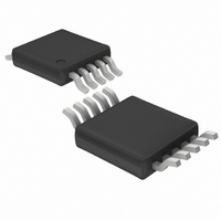
LTC1871EMS-1#PBF Linear Technology, LTC1871EMS-1#PBF Datasheet - Page 26

LTC1871EMS-1#PBF
Manufacturer Part Number
LTC1871EMS-1#PBF
Description
IC CONTRLR CURRENT MODE 10-MSOP
Manufacturer
Linear Technology
Type
Step-Up (Boost), Flyback, Sepicr
Datasheet
1.LTC1871EMS-1PBF.pdf
(36 pages)
Specifications of LTC1871EMS-1#PBF
Internal Switch(s)
No
Synchronous Rectifier
No
Number Of Outputs
1
Voltage - Output
1.23 ~ 72 V
Current - Output
50mA
Frequency - Switching
50kHz ~ 1MHz
Voltage - Input
2.5 ~ 36 V
Operating Temperature
-40°C ~ 85°C
Mounting Type
Surface Mount
Package / Case
10-MSOP, Micro10™, 10-uMAX, 10-uSOP
Lead Free Status / RoHS Status
Lead free / RoHS Compliant
Power - Output
-
Available stocks
Company
Part Number
Manufacturer
Quantity
Price
LTC1871-1
APPLICATIONS INFORMATION
devices are limited to 30V or less. Check the switching
waveforms directly across the drain and source terminals
of the power MOSFET to ensure the V
the maximum rating for the device.
During the MOSFET’s on-time, the control circuit limits
the maximum voltage drop across the power MOSFET to
about 150mV (at low duty cycle). The peak inductor current
is therefore limited to 150mV/R
between the maximum load current, duty cycle and the
R
The V
and is reduced to about 100mV at a duty cycle of 92% due
to slope compensation, as shown in Figure 8. The constant
‘χ’ in the denominator represents the ripple current in the
inductors relative to their maximum current. For example,
if 30% ripple current is chosen, then χ = 0.30. The ρ
accounts for the temperature coeffi cient of the R
the MOSFET, which is typically 0.4%/°C. Figure 9 illustrates
the variation of normalized R
a typical power MOSFET.
Another method of choosing which power MOSFET to
use is to check what the maximum output current is for a
given R
in discrete values.
Calculating Power MOSFET Switching and Conduction
Losses and Junction Temperatures
In order to calculate the junction temperature of the
power MOSFET, the power dissipated by the device must
be known. This power dissipation is a function of the
duty cycle, the load current and the junction temperature
itself. As a result, some iterative calculation is normally
required to determine a reasonably accurate value. Since
the controller is using the MOSFET as both a switching
and a sensing element, care should be taken to ensure
I
26
R
O(MAX)
DS(ON)
DS(ON)
SENSE(MAX)
DS(ON)
of the power MOSFET is:
V
V
SENSE(MAX)
SENSE(MAX)
R
I
DS(ON)
O(MAX)
since MOSFET on-resistances are available
term is typically 150mV at low duty cycle
•
•
1+
1+
2
DS(ON)
2
1
1
•
DS(ON)
•
T
T
over temperature for
•
•
DS
. The relationship
V
V
V
V
IN(MIN)
O
IN(MIN)
O
remains below
+ V
+ V
1
1
D
D
DS(ON)
+ 1
+ 1
T
term
of
that the converter is capable of delivering the required
load current over all operating conditions (load, line and
temperature) and for the worst-case specifi cations for
V
manufacturer’s data sheet.
The power dissipated by the MOSFET in a SEPIC converter
is:
The fi rst term in the equation above represents the I
losses in the device and the second term, the switching
losses. The constant k = 1.7 is an empirical factor inversely
related to the gate drive current and has the dimension
of 1/current.
From a known power dissipated in the power MOSFET, its
junction temperature can be obtained using the following
formula:
The R
the R
the board to the ambient temperature in the enclosure.
This value of T
assumption for the junction temperature in the iterative
calculation process.
SEPIC Converter: Output Diode Selection
To maximize effi ciency, a fast-switching diode with low
forward drop and low reverse leakage is desired. The output
diode in a SEPIC converter conducts current during the
switch off-time. The peak reverse voltage that the diode
must withstand is equal to V
forward current in normal operation is equal to the output
current, and the peak current is equal to:
The power dissipated by the diode is:
P
+ k • V
FET
SENSE(MAX)
T
P
I
D(PEAK)
J
D
= I
(
TH(JC)
= T
TH(JA)
= I
IN(MIN)
O(MAX)
A
O(MAX)
+ P
= 1+
for the device plus the thermal resistance from
to be used in this equation normally includes
and the R
FET
+ V
J
•
• V
1– D
O
can then be used to check the original
•R
2
D
)
D
1.85
TH(JA)
MAX
•I
MAX
DS(ON)
O(MAX)
•I
O(MAX)
2
• R
of the MOSFET listed in the
•
IN(MAX)
DS(ON)
•
V
V
O
IN(MIN)
1– D
D
+ V
MAX
• D
+ V
MAX
D
MAX
+ 1
O
. The average
• C
•
RSS
T
• f
18711fb
2
R


