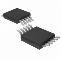
LTC1871EMS-1#PBF Linear Technology, LTC1871EMS-1#PBF Datasheet - Page 25

LTC1871EMS-1#PBF
Manufacturer Part Number
LTC1871EMS-1#PBF
Description
IC CONTRLR CURRENT MODE 10-MSOP
Manufacturer
Linear Technology
Type
Step-Up (Boost), Flyback, Sepicr
Datasheet
1.LTC1871EMS-1PBF.pdf
(36 pages)
Specifications of LTC1871EMS-1#PBF
Internal Switch(s)
No
Synchronous Rectifier
No
Number Of Outputs
1
Voltage - Output
1.23 ~ 72 V
Current - Output
50mA
Frequency - Switching
50kHz ~ 1MHz
Voltage - Input
2.5 ~ 36 V
Operating Temperature
-40°C ~ 85°C
Mounting Type
Surface Mount
Package / Case
10-MSOP, Micro10™, 10-uMAX, 10-uSOP
Lead Free Status / RoHS Status
Lead free / RoHS Compliant
Power - Output
-
Available stocks
Company
Part Number
Manufacturer
Quantity
Price
APPLICATIONS INFORMATION
The constant ‘χ’ represents the fraction of ripple current in
the inductor relative to its maximum value. For example, if
30% ripple current is chosen, then χ = 0.30 and the peak
current is 15% greater than the average.
It is worth noting here that SEPIC converters that operate
at high duty cycles (i.e., that develop a high output volt-
age from a low input voltage) can have very high input
currents, relative to the output current. Be sure to check
that the maximum load current will not overload the input
supply.
SEPIC Converter: Inductor Selection
For most SEPIC applications the equal inductor values
will fall in the range of 10μH to 100μH. Higher values will
reduce the input ripple voltage and reduce the core loss.
Lower inductor values are chosen to reduce physical size
and improve transient response.
Like the boost converter, the input current of the SEPIC
converter is calculated at full load current and minimum
input voltage. The peak inductor current can be signifi cantly
higher than the output current, especially with smaller in-
ductors and lighter loads. The following formulas assume
CCM operation and calculate the maximum peak inductor
currents at minimum V
The ripple current in the inductor is typically 20% to 40%
(i.e., a range of ‘χ’ from 0.20 to 0.40) of the maximum
average input current occurring at V
ΔI
the output current results in the following equations for
calculating the inductor value:
where:
L1
I
I
L =
L1(PEAK)
L2(PEAK)
= ΔI
I
L
V
= •I
IN(MIN)
L2
I
L
. Expressing this ripple current as a function of
= 1+
• f
= 1+
O(MAX)
• D
MAX
2
2
•
1– D
•I
•I
D
IN
O(MAX)
O(MAX)
MAX
:
MAX
•
•
V
V
V
O
IN(MIN)
IN(MIN)
IN(MIN)
V
+ V
IN(MIN)
D
+ V
and I
D
O(MAX)
and
By making L1 = L2 and winding them on the same core,
the value of inductance in the equation above is replace
by 2L due to mutual inductance. Doing this maintains the
same ripple current and energy storage in the inductors. For
example, a Coiltronix CTX10-4 is a 10μH inductor with two
windings. With the windings in parallel, 10μH inductance is
obtained with a current rating of 4A (the number of turns
hasn’t changed, but the wire diameter has doubled). Split-
ting the two windings creates two 10μH inductors with a
current rating of 2A each. Therefore, substituting 2L yields
the following equation for coupled inductors:
Specify the maximum inductor current to safely handle
I
current rating for the inductor should be checked at the
minimum input voltage (which results in the highest
inductor current) and maximum output current.
SEPIC Converter: Power MOSFET Selection
The power MOSFET serves two purposes in the LTC1871-1:
it represents the main switching element in the power path,
and its R
for the control loop. Important parameters for the power
MOSFET include the drain-to-source breakdown voltage
(BV
(R
and gate-to-drain charges (Q
the maximum drain current (I
thermal resistances (R
The gate drive voltage is set by the 5.2V INTV
regulator. Consequently, logic-level threshold MOSFETs
should be used in most LTC1871-1 applications. If low
input voltage operation is expected (e.g., supplying power
from a lithium-ion battery), then sublogic-level threshold
MOSFETs should be used.
The maximum voltage that the MOSFET switch must
sustain during the off-time in a SEPIC converter is equal
to the sum of the input and output voltages (V
As a result, careful attention must be paid to the BV
specifi cations for the MOSFETs relative to the maximum
actual switch voltage in the application. Many logic-level
L(PK)
DS(ON)
L1= L2 =
DSS
specifi ed in the equation above. The saturation
), the threshold voltage (V
) versus gate-to-source voltage, the gate-to-source
DS(ON)
2 • I
V
IN(MIN)
represents the current sensing element
L
• f
• D
TH(JC)
MAX
and R
GS
D(MAX)
GS(TH)
and Q
TH(JA)
LTC1871-1
) and the MOSFET’s
), the on-resistance
GD
).
, respectively),
CC
low dropout
O
25
+ V
18711fb
DSS
IN
).


