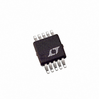
LT3758EMSE#PBF Linear Technology, LT3758EMSE#PBF Datasheet - Page 17

LT3758EMSE#PBF
Manufacturer Part Number
LT3758EMSE#PBF
Description
IC CTRLR DC/DC ADJ 10-MSOP
Manufacturer
Linear Technology
Type
Step-Up (Boost), Inverting, Flyback, Sepicr
Datasheet
1.LT3758EMSEPBF.pdf
(36 pages)
Specifications of LT3758EMSE#PBF
Internal Switch(s)
No
Synchronous Rectifier
No
Number Of Outputs
1
Frequency - Switching
100kHz ~ 1MHz
Voltage - Input
5.5 ~ 100 V
Operating Temperature
-40°C ~ 125°C
Mounting Type
Surface Mount
Package / Case
10-MSOP Exposed Pad, 10-HMSOP, 10-eMSOP
Dc To Dc Converter Type
FLYBACK CONTROLLER
Pin Count
10
Input Voltage
5.5 to 100V
Output Voltage
1.6 to 100V
Package Type
MSOP EP
Mounting
Surface Mount
Operating Temperature Classification
Automotive
Operating Temperature (min)
-40C
Operating Temperature (max)
125C
Lead Free Status / RoHS Status
Lead free / RoHS Compliant
Current - Output
-
Voltage - Output
-
Power - Output
-
Lead Free Status / Rohs Status
Compliant
Available stocks
Company
Part Number
Manufacturer
Quantity
Price
APPLICATIONS INFORMATION
The R
R
to the ambient temperature in the enclosure. T
exceed the diode maximum junction temperature rating.
Boost Converter: Output Capacitor Selection
Contributions of ESR (equivalent series resistance), ESL
(equivalent series inductance) and the bulk capacitance
must be considered when choosing the correct output
capacitors for a given output ripple voltage. The effect of
these three parameters (ESR, ESL and bulk C) on the output
voltage ripple waveform for a typical boost converter is
illustrated in Figure 6.
The choice of component(s) begins with the maximum
acceptable ripple voltage (expressed as a percentage of
the output voltage), and how this ripple should be divided
between the ESR step ΔV
ΔV
2% for the maximum output ripple, to be divided equally
between ΔV
change, depending on the requirements of the application,
and the following equations can easily be modifi ed. For a
1% contribution to the total ripple voltage, the ESR of the
output capacitor can be determined using the following
equation:
For the bulk C component, which also contributes 1% to
the total ripple:
θJC
Figure 6. The Output Ripple Waveform of a Boost Converter
COUT
ESR
C
OUT
for the device plus the thermal resistance from the board
θJA
. For the purpose of simplicity, we will choose
COUT
V
(AC)
OUT
≥
to be used in this equation normally includes the
0 01
ESR
. •
≤
I
t
ON
O MAX
0 01
(
and ΔV
. •
I
V
D PEAK
(
OUT
t
V
OFF
)
V
ESR
OUT
•
COUT
)
f
ESR
V
COUT
and the charging/discharging
. This percentage ripple will
RINGING DUE TO
TOTAL INDUCTANCE
(BOARD + CAP)
3758 F06
J
must not
The output capacitor in a boost regulator experiences high
RMS ripple currents, as shown in Figure 6. The RMS ripple
current rating of the output capacitor can be determined
using the following equation:
Multiple capacitors are often paralleled to meet ESR require-
ments. Typically, once the ESR requirement is satisfi ed, the
capacitance is adequate for fi ltering and has the required
RMS current rating. Additional ceramic capacitors in par-
allel are commonly used to reduce the effect of parasitic
inductance in the output capacitor, which reduces high
frequency switching noise on the converter output.
Boost Converter: Input Capacitor Selection
The input capacitor of a boost converter is less critical than
the output capacitor, due to the fact that the inductor is
in series with the input, and the input current waveform
is continuous. The input voltage source impedance
determines the size of the input capacitor, which is typically
in the range of 10μF to 100μF. A low ESR capacitor is
recommended, although it is not as critical as for the
output capacitor.
The RMS input capacitor ripple current for a boost con-
verter is:
FLYBACK CONVERTER APPLICATIONS
The LT3758 can be confi gured as a fl yback converter for the
applications where the converters have multiple outputs,
high output voltages or isolated outputs. Figure 7 shows
a simplifi ed fl yback converter.
The fl yback converter has a very low parts count for multiple
outputs, and with prudent selection of turns ratio, can
have high output/input voltage conversion ratios with a
desirable duty cycle. However, it has low effi ciency due to
the high peak currents, high peak voltages and consequent
power loss. The fl yback converter is commonly used for
an output power of less than 50W.
I
I
RMS(CIN)
RMS COUT
(
= 0.3 • ΔI
)
≥
I
O MAX
(
L
)
•
− 1
D
MAX
D
MAX
LT3758
17
3758fb


