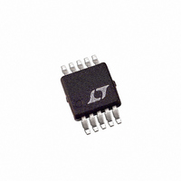
LT3758EMSE#PBF Linear Technology, LT3758EMSE#PBF Datasheet - Page 25

LT3758EMSE#PBF
Manufacturer Part Number
LT3758EMSE#PBF
Description
IC CTRLR DC/DC ADJ 10-MSOP
Manufacturer
Linear Technology
Type
Step-Up (Boost), Inverting, Flyback, Sepicr
Datasheet
1.LT3758EMSEPBF.pdf
(36 pages)
Specifications of LT3758EMSE#PBF
Internal Switch(s)
No
Synchronous Rectifier
No
Number Of Outputs
1
Frequency - Switching
100kHz ~ 1MHz
Voltage - Input
5.5 ~ 100 V
Operating Temperature
-40°C ~ 125°C
Mounting Type
Surface Mount
Package / Case
10-MSOP Exposed Pad, 10-HMSOP, 10-eMSOP
Dc To Dc Converter Type
FLYBACK CONTROLLER
Pin Count
10
Input Voltage
5.5 to 100V
Output Voltage
1.6 to 100V
Package Type
MSOP EP
Mounting
Surface Mount
Operating Temperature Classification
Automotive
Operating Temperature (min)
-40C
Operating Temperature (max)
125C
Lead Free Status / RoHS Status
Lead free / RoHS Compliant
Current - Output
-
Voltage - Output
-
Power - Output
-
Lead Free Status / Rohs Status
Compliant
Available stocks
Company
Part Number
Manufacturer
Quantity
Price
APPLICATIONS INFORMATION
Check the stress on the power MOSFET by measuring its
drain-to-source voltage directly across the device terminals
(reference the ground of a single scope probe directly to
the source pad on the PC board). Beware of inductive
ringing, which can exceed the maximum specifi ed voltage
rating of the MOSFET. If this ringing cannot be avoided,
and exceeds the maximum rating of the device, either
choose a higher voltage device or specify an avalanche-
rated power MOSFET.
The small-signal components should be placed away
from high frequency switching nodes. For optimum load
VIAS TO GROUND
PLANE
C
C
R1
R2
C
R
C1
C2
SS
T
R
C
1
2
3
4
5
Figure 11. Suggested Layout of the 10V to 40V Input, 48V Output
Boost Converter in the Typical Applications Section
LT3758
10
9
8
7
6
C
C
OUT2
IN
R3
C
R
VCC
S
1
2
3
4
C
OUT1
regulation and true remote sensing, the top of the output
voltage sensing resistor divider should connect indepen-
dently to the top of the output capacitor (Kelvin connec-
tion), staying away from any high dV/dt traces. Place the
divider resistors near the LT3758 in order to keep the high
impedance FBX node short.
Figure 11 shows the suggested layout of the 10V to 40V
input, 48V output boost converter in the Typical Applica-
tions section.
M1
8
7
6
5
D1
L1
3758 F11
V
V
IN
OUT
LT3758
25
3758fb


