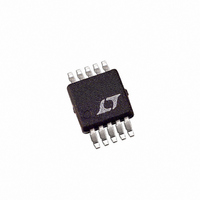
LT3758EMSE#PBF Linear Technology, LT3758EMSE#PBF Datasheet - Page 19

LT3758EMSE#PBF
Manufacturer Part Number
LT3758EMSE#PBF
Description
IC CTRLR DC/DC ADJ 10-MSOP
Manufacturer
Linear Technology
Type
Step-Up (Boost), Inverting, Flyback, Sepicr
Datasheet
1.LT3758EMSEPBF.pdf
(36 pages)
Specifications of LT3758EMSE#PBF
Internal Switch(s)
No
Synchronous Rectifier
No
Number Of Outputs
1
Frequency - Switching
100kHz ~ 1MHz
Voltage - Input
5.5 ~ 100 V
Operating Temperature
-40°C ~ 125°C
Mounting Type
Surface Mount
Package / Case
10-MSOP Exposed Pad, 10-HMSOP, 10-eMSOP
Dc To Dc Converter Type
FLYBACK CONTROLLER
Pin Count
10
Input Voltage
5.5 to 100V
Output Voltage
1.6 to 100V
Package Type
MSOP EP
Mounting
Surface Mount
Operating Temperature Classification
Automotive
Operating Temperature (min)
-40C
Operating Temperature (max)
125C
Lead Free Status / RoHS Status
Lead free / RoHS Compliant
Current - Output
-
Voltage - Output
-
Power - Output
-
Lead Free Status / Rohs Status
Compliant
Available stocks
Company
Part Number
Manufacturer
Quantity
Price
APPLICATIONS INFORMATION
Flyback Converter: Transformer Design for
Discontinuous Mode Operation
The transformer design for discontinuous mode of opera-
tion is chosen as presented here. According to Figure 8,
the minimum D3 (D3
has the minimum V
(P
to guarantee the converter is always in discontinuous
mode operation. Choosing higher D3 allows the use of
low inductances but results in higher switch peak current.
The user can choose a D
maximum average primary currents can be calculated by
the following equation:
where η is the converter effi ciency.
If the fl yback converter has multiple outputs, P
is the sum of all the output power.
The maximum average secondary current is:
where
D2 = 1 – D
the primary and secondary RMS currents are:
According to Figure 8, the primary and secondary peak
currents are:
OUT
I
I
I
I
I
I
LP(PEAK)
LS(PEAK)
LP MAX
LS MAX
LP RMS
LS RMS
). Choose D3
(
(
(
(
)
)
)
)
MAX
=
=
=
=
= I
= I
I
I
2
2
D MAX
SW MAX
SW(PEAK)
D(PEAK)
(
•
•
– D3
I
I
LP MAX
LS MAX
(
MIN
(
(
)
IN
MIN
=
)
= 2 • I
to be equal to or higher than 10%
=
I
and the maximum output power
) )
OUT MAX
)
= 2 • I
) occurs when the the converter
MAX
D
•
•
MAX
D
(
2
D2
LS(MAX)
D
as the start point. Then, the
P
3
LP(MAX)
MAX
OUT MAX
3
•
)
V
IN MIN
(
(
)
)
•
η
OUT(MAX)
The primary and second inductor values of the fl yback
converter transformer can be determined using the fol-
lowing equations:
The primary to second turns ratio is:
Flyback Converter: Snubber Design
Transformer leakage inductance (on either the primary or
secondary) causes a voltage spike to occur after the MOS-
FET turn-off. This is increasingly prominent at higher load
currents, where more stored energy must be dissipated.
In some cases a snubber circuit will be required to avoid
overvoltage breakdown at the MOSFET’s drain node. There
are different snubber circuits, and Application Note 19 is
a good reference on snubber design. An RCD snubber is
shown in Figure 7.
The snubber resistor value (R
following equation:
where V
V
2 to 2.5 times of:
SN
L
L
R
N
N
V
P
S
results in a larger snubber loss. A reasonable V
SN
P
S
OUT
=
=
=
N
=
D
D
SN
S
2
2
2
2
•
MAX
L
L
N
2
2
•
•
is the snubber capacitor voltage. A smaller
I
P
S
P
•(
•
OUT MAX
V
P
V
OUT MAX
2
•
I
O
SN
2
(
V
U U T
SW PEAK
2
(
IN MAX
−
+
(
(
)
V
V
•
SN
)
D
f
•
)
•
)
)
f
•
V
•
L
η
OUT
SN
LK
) can be calculated by the
•
•
N
N
f
P
S
LT3758
19
SN
3758fb
is


