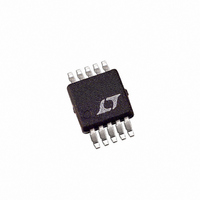
LT3758EMSE#PBF Linear Technology, LT3758EMSE#PBF Datasheet - Page 21

LT3758EMSE#PBF
Manufacturer Part Number
LT3758EMSE#PBF
Description
IC CTRLR DC/DC ADJ 10-MSOP
Manufacturer
Linear Technology
Type
Step-Up (Boost), Inverting, Flyback, Sepicr
Datasheet
1.LT3758EMSEPBF.pdf
(36 pages)
Specifications of LT3758EMSE#PBF
Internal Switch(s)
No
Synchronous Rectifier
No
Number Of Outputs
1
Frequency - Switching
100kHz ~ 1MHz
Voltage - Input
5.5 ~ 100 V
Operating Temperature
-40°C ~ 125°C
Mounting Type
Surface Mount
Package / Case
10-MSOP Exposed Pad, 10-HMSOP, 10-eMSOP
Dc To Dc Converter Type
FLYBACK CONTROLLER
Pin Count
10
Input Voltage
5.5 to 100V
Output Voltage
1.6 to 100V
Package Type
MSOP EP
Mounting
Surface Mount
Operating Temperature Classification
Automotive
Operating Temperature (min)
-40C
Operating Temperature (max)
125C
Lead Free Status / RoHS Status
Lead free / RoHS Compliant
Current - Output
-
Voltage - Output
-
Power - Output
-
Lead Free Status / Rohs Status
Compliant
Available stocks
Company
Part Number
Manufacturer
Quantity
Price
APPLICATIONS INFORMATION
Flyback Converter: Input Capacitor Selection
The input capacitor in a fl yback converter is subject to
a large RMS current due to the discontinuous primary
current. To prevent large voltage transients, use a low
ESR input capacitor sized for the maximum RMS current.
The RMS ripple current rating of the input capacitors in
discontinuous operation can be determined using the
following equation:
SEPIC CONVERTER APPLICATIONS
The LT3758 can be confi gured as a SEPIC (single-ended
primary inductance converter), as shown in Figure 1. This
topology allows for the input to be higher, equal, or lower
than the desired output voltage. The conversion ratio as
a function of duty cycle is:
in continuous conduction mode (CCM).
In a SEPIC converter, no DC path exists between the input
and output. This is an advantage over the boost converter
for applications requiring the output to be disconnected
from the input source when the circuit is in shutdown.
Compared to the fl yback converter, the SEPIC converter
has the advantage that both the power MOSFET and the
output diode voltages are clamped by the capacitors (C
C
across the power MOSFET and the output diodes. The
SEPIC converter requires much smaller input capacitors
than those of the fl yback converter. This is due to the fact
that, in the SEPIC converter, the inductor L1 is in series
with the input, and the ripple current fl owing through the
input capacitor is continuous.
SEPIC Converter: Switch Duty Cycle and Frequency
For a SEPIC converter operating in CCM, the duty cycle
of the main switch can be calculated based on the output
voltage (V
forward voltage (V
DC
I
RMS CIN DISCONTINUOUS
V
OUT
and C
V
(
IN
+
),
OUT
V
OUT
D
=
), the input voltage (V
), therefore, there is less voltage ringing
− 1
D
D
D
).
≥
V
P
IN MIN
OUT MAX
(
(
)
•
η
)
IN
• •
) and the diode
4
−
3
( •
•
3
D
MAX
D
MAX
)
IN
,
The maximum duty cycle (D
has the minimum input voltage:
SEPIC Converter: Inductor and Sense Resistor Selection
As shown in Figure 1, the SEPIC converter contains two
inductors: L1 and L2. L1 and L2 can be independent, but
can also be wound on the same core, since identical volt-
ages are applied to L1 and L2 throughout the switching
cycle.
For the SEPIC topology, the current through L1 is the
converter input current. Based on the fact that, ideally, the
output power is equal to the input power, the maximum
average inductor currents of L1 and L2 are:
In a SEPIC converter, the switch current is equal to I
I
average switch current is defi ned as:
and the peak switch current is:
The constant χ in the preceding equations represents
the percentage peak-to-peak ripple current in the switch,
relative to I
ripple current ΔI
The inductor ripple currents ΔI
The inductor ripple current has a direct effect on the
choice of the inductor value. Choosing smaller values of
L2
ΔI
ΔI
I
I
I
I
D
when the power switch is on, therefore, the maximum
L MAX
L MAX
SW MAX
SW PEAK
MAX
1
2
SW
L1
(
(
(
(
= ΔI
= χ • I
=
)
) )
SW(MAX)
=
V
)
=I
)
L2
=
IN MIN
I
=
IN MAX
O MAX
I
(
SW(MAX)
L MAX
= 0.5 • ΔI
⎛
⎝ ⎜
(
(
1
V
1
SW
(
+
OUT
)
, as shown in Figure 9. Then, the switch
+
χ
2
can be calculated by:
)
)
=
V
)
⎞
⎠ ⎟
+
+
OUT
I
•
O MAX
V
I
I
SW
(
O MAX
L MAX
D
2
(
MAX
+
(
V
)
) occurs when the converter
D
•
L1
)
)
1
•
=
−
and ΔI
1
D
I
−
MAX
D
O MAX
D
MAX
(
1
MAX
L2
)
•
LT3758
are identical:
1
−
D
1
MAX
21
3758fb
L1
+


