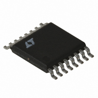
LT3825EFE#TRPBF Linear Technology, LT3825EFE#TRPBF Datasheet - Page 10

LT3825EFE#TRPBF
Manufacturer Part Number
LT3825EFE#TRPBF
Description
IC CNTRLR SYNC 16-TSSOP
Manufacturer
Linear Technology
Type
Flybackr
Datasheet
1.LT3825EFEPBF.pdf
(32 pages)
Specifications of LT3825EFE#TRPBF
Internal Switch(s)
No
Synchronous Rectifier
Yes
Number Of Outputs
1
Frequency - Switching
50kHz ~ 250kHz
Voltage - Input
12 ~ 18 V
Operating Temperature
-40°C ~ 125°C
Mounting Type
Surface Mount
Package / Case
16-TSSOP Exposed Pad, 16-eTSSOP, 16-HTSSOP
Power - Output
60W
Lead Free Status / RoHS Status
Lead free / RoHS Compliant
Current - Output
-
Voltage - Output
-
Available stocks
Company
Part Number
Manufacturer
Quantity
Price
LT3825
OPERATION
The LT3825 is a current mode switcher controller IC de-
signed specifi cally for use in an isolated fl yback topology
employing synchronous rectifi cation. The LT3825 operation
is similar to traditional current mode switchers. The major
difference is that output voltage feedback is derived via
sensing the output voltage through the transformer. This
precludes the need of an optoisolator in isolated designs
greatly improving dynamic response and reliability. The
LT3825 has a unique feedback amplifi er that samples a
transformer winding voltage during the fl yback period and
uses that voltage to control output voltage.
The internal blocks are similar to many current mode
controllers. The differences lie in the fl yback feedback
amplifi er and load compensation circuitry. The logic block
also contains circuitry to control the special dynamic
requirements of fl yback control.
For more information on the basics of current mode
switcher/controllers and isolated fl yback converters see
Application Note 19.
Feedback Amplifi er—Pseudo DC Theory
For the following discussion refer to the simplifi ed Fly-
back Feedback Amplifi er diagram. When the primary-side
MOSFET switch MP turns off, its drain voltage rises above
the V
off and the synchronous secondary MOSFET is on. Dur-
ing fl yback the voltage on nondriven transformer pins is
determined by the secondary voltage. The amplitude of this
fl yback pulse as seen on the third winding is given as:
R
I
ESR = impedance of secondary circuit capacitor, winding
and traces
N
turns ratio (i.e., N
The fl yback voltage is scaled by an external resistive divider
R1/R2 and presented at the FB pin. The feedback amplifi er
10
SEC
DS(ON)
SF
V
= transformer effective secondary-to-feedback winding
= transformer secondary current
FLBK
IN
rail. Flyback occurs when the primary MOSFET is
= on-resistance of the synchronous MOSFET M
=
V
OUT
S
+
/N
I
SEC
FLBK
•
)
N
(
ESR R
SF
+
DS ON
(
)
)
S
compares the voltage to the internal bandgap reference.
The feedback amp is actually a transconductance ampli-
fi er whose output is connected to V
in the fl yback time. An external capacitor on the V
integrates the net feedback amp current to provide the
control voltage to set the current mode trip point.
The regulation voltage at the FB pin is nearly equal to the
bandgap reference V
overall loop. The relationship between V
expressed as:
Combining this with the previous V
an expression for V
programming resistors and secondary resistances:
The effect of nonzero secondary output impedance is dis-
cussed in further detail; see Load Compensation Theory.
The practical aspects of applying this equation for V
are found in the Applications Information.
Feedback Amplifi er Dynamic Theory
So far, this has been a pseudo-DC treatment of fl yback
feedback amplifi er operation. But the fl yback signal is a
pulse, not a DC level. Provision must be made to enable
the fl yback amplifi er only when the fl yback pulse is present.
This is accomplished by the “Enable” line in the diagram.
Timing signals are then required to enable and disable the
fl yback amplifi er. There are several timing signals which
are required for proper LT3825 operation. Please refer to
the Timing Diagram.
Minimum Output Switch On-Time (t
The LT3825 affects output voltage regulation via fl yback
pulse action. If the output switch is not turned on, there
is no fl yback pulse and output voltage information is
not available. This causes irregular loop response and
start-up/latch-up problems. The solution is to require the
primary switch to be on for an absolute minimum time
per each oscillator cycle. If the output load is less than
V
OUT
V
FLBK
=
⎛
⎜
⎝
R1+ R2
=
R2
R
1
R
+
2
R
• V
2
OUT
•
FB
FB
V
FB
in terms of the internal reference,
• N
because of the high gain in the
SF
⎞
⎟ – I
⎠
SEC
FLBK
C
only during a period
ON(MIN)
• ESR + R
(
expression yields
FLBK
)
and V
DS(ON)
C
FB
3525fc
OUT
pin
)
is


