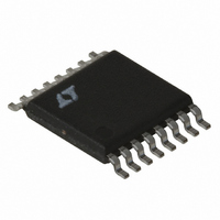
LT3825EFE#TRPBF Linear Technology, LT3825EFE#TRPBF Datasheet - Page 22

LT3825EFE#TRPBF
Manufacturer Part Number
LT3825EFE#TRPBF
Description
IC CNTRLR SYNC 16-TSSOP
Manufacturer
Linear Technology
Type
Flybackr
Datasheet
1.LT3825EFEPBF.pdf
(32 pages)
Specifications of LT3825EFE#TRPBF
Internal Switch(s)
No
Synchronous Rectifier
Yes
Number Of Outputs
1
Frequency - Switching
50kHz ~ 250kHz
Voltage - Input
12 ~ 18 V
Operating Temperature
-40°C ~ 125°C
Mounting Type
Surface Mount
Package / Case
16-TSSOP Exposed Pad, 16-eTSSOP, 16-HTSSOP
Power - Output
60W
Lead Free Status / RoHS Status
Lead free / RoHS Compliant
Current - Output
-
Voltage - Output
-
Available stocks
Company
Part Number
Manufacturer
Quantity
Price
APPLICATIONS INFORMATION
LT3825
Output Voltage Error Sources
The LT3825’s feedback sensing introduces additional
sources of errors. The following is a summary list.
The internal bandgap voltage reference sets the reference
voltage for the feedback amplifier. The specifications detail
its variation.
The external feedback resistive divider ratio proportional
directly affects regulated voltage. Use 1% components.
Leakage inductance on the transformer secondary reduces
the effective secondary-to-feedback winding turns ratio
(N
age target by a similar percentage. Since secondary leakage
inductance is constant from part to part (with a tolerance)
adjust the feedback resistor ratio to compensate.
The transformer secondary current flows through the
impedances of the winding resistance, synchronous MOS-
FET R
current for these errors is higher than the load current
because conduction occurs only during the converter’s
“off” time. So divide the load current by (1 – DC).
If the output load current is relatively constant, the feedback
resistive divider is used to compensate for these losses.
Otherwise, use the LT3825 load compensation circuitry
(see Load Compensation).
If multiple output windings are used, the flyback winding will
have a signal that represents an amalgamation of all these
windings impedances. Take care that you examine worst-
case loading conditions when tweaking the voltages.
Power MOSFET Selection
The power MOSFETs are selected primarily on the criteria of
on- resistance, R
breakdown voltage (BV
and maximum drain current (I
22
S
/N
F
DS(ON)
) from its ideal value. This increases the output volt-
and output capacitor ESR. The DC equivalent
DS(ON)
, input capacitance, drain-to-source
DSS
), maximum gate voltage (V
D(MAX)
).
GS
)
For the primary-side power MOSFET, the peak current is:
where X
earlier.
For each secondary-side power MOSFET, the peak current
is:
Select a primary-side power MOSFET with a BV
than:
where N
mary winding. L
and C
C
be added to reduce the leakage inductance as discussed
earlier.
For each secondary-side power MOSFET, the BV
be greater than:
Choose the primary-side MOSFET R
gate drive voltage (7.5V). The secondary side MOSFET gate
drive voltage depends on the gate drive method.
Primary-side power MOSFET RMS current is given by:
OSS
BV
I
I
BV
I
PK(PRI)
PK(SEC)
RMS PRI
of the primary-side power MOSFET). A snubber may
DSS
DSS
P
(
is the primary-side capacitance (mostly from the
SP
MIN
≥ V
≥I
reflects the turns ratio of that secondary-to-pri-
=
)
=
PK
=
OUT
V
is peak-to-peak current ratio as defined
1– DC
IN(MIN)
V
LKG
IN MIN
I
L
OUT
+ V
(
C
LKG
is the primary-side leakage inductance
P
MAX
P
IN(MAX)
IN
• DC
P
)
+ V
IN
DC
• 1+
IN(MAX)
MAX
⎛
⎜
⎝
MAX
• N
X
• 1+
SP
MIN
⎛
⎜
⎝
2
+
V
DS(ON)
⎞
⎟
⎠
OUT(MAX)
X
MIN
N
2
SP
⎞
⎟
⎠
at the nominal
DSS
DSS
greater
should
3525fc


