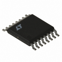
LT3825EFE#TRPBF Linear Technology, LT3825EFE#TRPBF Datasheet - Page 18

LT3825EFE#TRPBF
Manufacturer Part Number
LT3825EFE#TRPBF
Description
IC CNTRLR SYNC 16-TSSOP
Manufacturer
Linear Technology
Type
Flybackr
Datasheet
1.LT3825EFEPBF.pdf
(32 pages)
Specifications of LT3825EFE#TRPBF
Internal Switch(s)
No
Synchronous Rectifier
Yes
Number Of Outputs
1
Frequency - Switching
50kHz ~ 250kHz
Voltage - Input
12 ~ 18 V
Operating Temperature
-40°C ~ 125°C
Mounting Type
Surface Mount
Package / Case
16-TSSOP Exposed Pad, 16-eTSSOP, 16-HTSSOP
Power - Output
60W
Lead Free Status / RoHS Status
Lead free / RoHS Compliant
Current - Output
-
Voltage - Output
-
Available stocks
Company
Part Number
Manufacturer
Quantity
Price
APPLICATIONS INFORMATION
LT3825
The t
Keep R
is 160k.
Enable Delay Time (ENDLY)
Enable delay time provides a programmable delay between
turn-off of the primary gate drive node and the subsequent
enabling of the feedback amplifier. As discussed earlier, this
delay allows the feedback amplifier to ignore the leakage
inductance voltage spike on the primary side.
The worst-case leakage spike pulse width is at maximum
load conditions. So set the enable delay time at these
conditions.
While the typical applications for this part use forced
continuous operation, it is conceivable that a secondary-
side controller might cause discontinuous operation at
light loads. Under such conditions the amount of energy
stored in the transformer is small. The flyback waveform
becomes “lazy” and some time elapses before it indicates
the actual secondary output voltage. The enable delay time
should be made long enough to ignore the “irrelevant”
portion of the flyback waveform at light load.
Even though the LT3825 has a robust gate drive, the gate
transition time slows with very large MOSFETs. Increase
delay time as required when using such MOSFETs.
The enable delay resistor is set with the following
equation:
Keep R
56k.
Primary Gate Delay Time (PGDLY)
Primary gate delay is the programmable time from the
turn-off of the synchronous MOSFET to the turn-on of the
primary-side MOSFET. Correct setting eliminates overlap
18
R
R
ENDLY
tON(MIN)
ON(MIN)
tON(MIN)
ENDLY
(kΩ) =
(kΩ) =
resistor is set with the following equation:
greater than 40k. A good starting point is
greater than 70k. A good starting value
t
ENDLY
t
ON(MIN)
2.616
(ns) – 30
1.063
(ns) – 104
between the primary-side switch and secondary-side syn-
chronous switch(es) and the subsequent current spike in
the transformer. This spike will cause additional component
stress and a loss in regulator efficiency.
The primary gate delay resistor is set with the following
equation:
A good starting point is 27k.
Soft-Start Functions
The LT3825 contains an optional soft-start function that is
enabled by connecting an external capacitor between the
SFST pin and ground. Internal circuitry prevents the control
voltage at the V
There is an initial pull-up circuit to quickly bring the SFST
voltage to approximately 0.8V. From there it charges to
approximately 2.8V with a 20μA current source.
The SFST node is discharged to 0.8V when a fault occurs.
A fault is V
voltage greater than 200mV or the IC’s thermal (over tem-
perature) shutdown is tripped. When SFST discharges, the
V
current voltage. Once discharged and the fault removed,
the SFST recharges up again.
In this manner, switch currents are reduced and the stresses
in the converter are reduced during fault conditions.
The time it takes to fully charge soft-start is:
UVLO Pin Function
The UVLO pin provides a user programming undervoltage
lockout. This is typically used to provide undervoltage
lockout based on V
UVLO is below the 1.24V UVLO threshold. An external
resistive divider between the input supply and ground is
used to set the turn-on voltage.
C
R
node voltage is also pulled low to below the minimum
t
SS
PGDLY
=
C
CC
SFST
(kΩ) =
too low (undervoltage lockout), current sense
20μA
C
• 1.4V
pin from exceeding that on the SFST pin.
t
IN
PGDLY
. The gate drivers are disabled when
= 70ms • C
9.01
(ns) + 47
SFST
(μF)
3525fc


