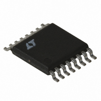
LT1976EFE Linear Technology, LT1976EFE Datasheet - Page 17

LT1976EFE
Manufacturer Part Number
LT1976EFE
Description
IC REG SW STEP DWN 1.5A 16-TSSOP
Manufacturer
Linear Technology
Type
Step-Down (Buck)r
Datasheet
1.LT1976IFEPBF.pdf
(28 pages)
Specifications of LT1976EFE
Internal Switch(s)
Yes
Synchronous Rectifier
No
Number Of Outputs
1
Voltage - Output
1.2 ~ 54 V
Current - Output
1.5A
Frequency - Switching
200kHz
Voltage - Input
3.3 ~ 60 V
Operating Temperature
-40°C ~ 125°C
Mounting Type
Surface Mount
Package / Case
16-TSSOP Exposed Pad, 16-eTSSOP, 16-HTSSOP
Lead Free Status / RoHS Status
Contains lead / RoHS non-compliant
Power - Output
-
Available stocks
Company
Part Number
Manufacturer
Quantity
Price
Part Number:
LT1976EFE
Manufacturer:
LINEAR/凌特
Quantity:
20 000
Company:
Part Number:
LT1976EFE#PBF
Manufacturer:
IR
Quantity:
120
Part Number:
LT1976EFE#PBF
Manufacturer:
LINEAR/凌特
Quantity:
20 000
Company:
Part Number:
LT1976EFE#TRPBF
Manufacturer:
LT
Quantity:
1 560
Part Number:
LT1976EFE#TRPBF
Manufacturer:
LTNEAR
Quantity:
20 000
APPLICATIO S I FOR ATIO
Short-Circuit Considerations
The LT1976 is a current mode controller. It uses the V
node voltage as an input to a current comparator which
turns off the output switch on a cycle-by-cycle basis as
this peak current is reached. The internal clamp on the V
node, nominally 2.2V, then acts as an output switch peak
current limit. This action becomes the switch current limit
specification. The maximum available output power is
then determined by the switch current limit.
A potential controllability prod}m could occur under short-
circuit conditions. If the power supply output is short
circuited, the feedback amplifier responds to the low
output voltage by raising the control voltage, V
peak current limit value. Ideally, the output switch would
be turned on, and then turned off as its current exceeded
the value indicated by V
time involved in both the current comparator and turn-off
of the output switch. These result in a minimum on time
t
(V
voltage drop, the potential exists for a loss of control.
Expressed mathematically the requirement to maintain
control is:
where:
If this condition is not observed, the current will not be
limited at I
higher value. Using the nominal LT1976 clock frequency
of 200kHz, a V
maximum t
90ns, an unacceptably short time.
ON(MIN).
F
f = switching frequency
t
V
V
I • R = inductor I • R voltage drop
f t
ON
+ I • R), the diode forward voltage plus inductor I • R
F
IN
•
= diode forward voltage
= switch on time
ON
= Input voltage
When combined with the large ratio of V
≤
PK
ON
V
F
but will cycle-by-cycle ratchet up to some
to maintain control would be approximately
IN
V
+
IN
of 40V and a (V
I R
•
U
C
. However, there is finite response
U
F
+ I • R) of say 0.7V, the
W
U
C
, to its
IN
to
C
C
The solution to this dilemma is to slow down the oscillator
to allow the current in the inductor to drop to a sufficiently
low value such that the current doesn’t continue to ratchet
higher. When the FB pin voltage is abnormally low thereby
indicating some sort of short-circuit condition, the oscil-
lator frequency will be reduced. Oscillator frequency is
reduced by a factor of 4 when the FB pin voltage is below
0.4V and increases linearly to its typical value of 200kHz at
a FB voltage of 0.95V (see Typical Performance Character-
istics). In addition, if the current in the switch exceeds 1.5
• I
the next on cycle effectively reducing the oscillator fre-
quency by a factor of 2. These oscillator frequency reduc-
tions during short-circuit conditions allow the LT1976 to
maintain current control.
SOFT-START
For applications where [V
large input surge currents can’t be tolerated, the LT1976
soft-start feature should be used to control the output
capacitor charge rate during start-up, or during recovery
from an output short circuit thereby adding additional
control over peak inductor current. The soft-start function
limits the switch current via the V
constant voltage ramp rate (dV/dt) at the output capacitor.
A capacitor (C1 in Figure 2) from the C
regulated output voltage determines the output voltage
ramp rate. When the current through the C
exceeds the C
output capacitor is limited by reducing the V
The C
Typical Performance Characteristics) and is defeated for
FB voltages greater than 0.9V (typical). The output dV/dt
can be approximated by:
but actual values will vary due to start-up load conditions,
compensation values and output capacitor selection.
PK
dV
dt
current demanded by the V
SS
=
threshold is proportional to the FB voltage (see
I
C
CSS
SS
SS
threshold (I
LT1976/LT1976B
IN
/(V
CSS
OUT
C
), the voltage ramp of the
pin, the LT1976 will skip
+ V
C
pin to maintain a
F
)] ratios > 10 or
SS
C
SS
pin voltage.
pin to the
capacitor
17
1976bfg


