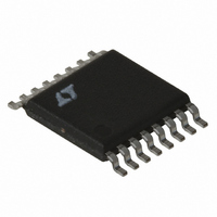
LT1976EFE Linear Technology, LT1976EFE Datasheet - Page 9

LT1976EFE
Manufacturer Part Number
LT1976EFE
Description
IC REG SW STEP DWN 1.5A 16-TSSOP
Manufacturer
Linear Technology
Type
Step-Down (Buck)r
Datasheet
1.LT1976IFEPBF.pdf
(28 pages)
Specifications of LT1976EFE
Internal Switch(s)
Yes
Synchronous Rectifier
No
Number Of Outputs
1
Voltage - Output
1.2 ~ 54 V
Current - Output
1.5A
Frequency - Switching
200kHz
Voltage - Input
3.3 ~ 60 V
Operating Temperature
-40°C ~ 125°C
Mounting Type
Surface Mount
Package / Case
16-TSSOP Exposed Pad, 16-eTSSOP, 16-HTSSOP
Lead Free Status / RoHS Status
Contains lead / RoHS non-compliant
Power - Output
-
Available stocks
Company
Part Number
Manufacturer
Quantity
Price
Part Number:
LT1976EFE
Manufacturer:
LINEAR/凌特
Quantity:
20 000
Company:
Part Number:
LT1976EFE#PBF
Manufacturer:
IR
Quantity:
120
Part Number:
LT1976EFE#PBF
Manufacturer:
LINEAR/凌特
Quantity:
20 000
Company:
Part Number:
LT1976EFE#TRPBF
Manufacturer:
LT
Quantity:
1 560
Part Number:
LT1976EFE#TRPBF
Manufacturer:
LTNEAR
Quantity:
20 000
C
output voltage determines the output voltage ramp rate
during start-up. When the current through the C
tor exceeds the C
the output is limited. The C
the FB voltage (see Typical Performance Characteristics)
and is defeated for FB voltage greater than 0.9V (typical).
See Soft-Start section in Applications Information for
details.
BIAS (Pin 10): The BIAS pin is used to improve efficiency
when operating at higher input voltages and light load
current. Connecting this pin to the regulated output volt-
age forces most of the internal circuitry to draw its
operating current from the output voltage rather than the
input supply. This architecture increases efficiency espe-
cially when the input voltage is much higher than the
output. Minimum output voltage setting for this mode of
operation is 3V.
V
and the input of the peak switch current comparator. It is
normally used for frequency compensation, but can also
serve as a current clamp or control loop override. The V
pin sits about 0.45V for light loads and 2.2V at current
limit. The LT1976 clamps the V
burst threshold during sleep periods for better transient
response. Driving the V
ing and also place the LT1976 into sleep mode.
FB (Pin 12): The feedback pin is used to determine the
output voltage using an external voltage divider from the
output that generates 1.25V at the FB pin . When the FB pin
drops below 0.9V, switching frequency is reduced, the
SYNC function is disabled and output ramp rate control is
enabled via the C
Applications Information for details.
PI FU CTIO S
SS
C
(Pin 11): The V
U
(Pin 9): A capacitor from the C
U
SS
C
SS
pin is the output of the error amplifier
threshold (I
U
pin. See the Feedback section in
C
pin to ground will disable switch-
SS
threshold is proportional to
CSS
C
SS
pin slightly below the
), the voltage ramp of
pin to the regulated
SS
capaci-
C
PGFB (PIN 13): The PGFB pin is the positive input to a
comparator whose negative input is set at V
PGFB is taken above V
the C
on the PGFB pin drops below V
discharged resetting the PG delay period. The PGFB volt-
age is typically generated by a resistive divider from the
regulated output or input supply. See Power Good section
in Applications Information for details.
SYNC (Pin 14): The SYNC pin is used to synchronize the
internal oscillator to an external signal. It is directly logic
compatible and can be driven with any signal between
20% and 80% duty cycle. The synchronizing range is
equal to maximum initial operating frequency up to 700kHz.
When the voltage on the FB pin is below 0.9V the SYNC
function is disabled. See the Synchronizing section in
Applications Information for details.
SHDN (Pin 15): The SHDN pin is used to turn off the
regulator and to reduce input current to less than 1μA. The
SHDN pin requires a voltage above 1.3V with a typical
source current of 5μA to take the IC out of the shutdown
state.
PG (Pin 16): The PG pin is functional only when the SHDN
pin is above its threshold, and is active low when the
internal clamp on the C
high impedance when the clamp is active. The PG pin has
a typical sink capability of 200μA. See the Power Good
section in Applications Information for details.
T
pin starting the PG delay period. When the voltage
PGFB
T
LT1976/LT1976B
pin is below its clamp level and
, current (I
PGFB
, the C
CSS
) is sourced into
T
pin is rapidly
PGFB
. When
1976bfg
9


