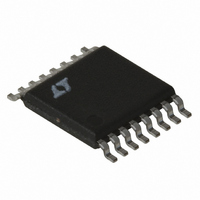
LT1976EFE Linear Technology, LT1976EFE Datasheet - Page 23

LT1976EFE
Manufacturer Part Number
LT1976EFE
Description
IC REG SW STEP DWN 1.5A 16-TSSOP
Manufacturer
Linear Technology
Type
Step-Down (Buck)r
Datasheet
1.LT1976IFEPBF.pdf
(28 pages)
Specifications of LT1976EFE
Internal Switch(s)
Yes
Synchronous Rectifier
No
Number Of Outputs
1
Voltage - Output
1.2 ~ 54 V
Current - Output
1.5A
Frequency - Switching
200kHz
Voltage - Input
3.3 ~ 60 V
Operating Temperature
-40°C ~ 125°C
Mounting Type
Surface Mount
Package / Case
16-TSSOP Exposed Pad, 16-eTSSOP, 16-HTSSOP
Lead Free Status / RoHS Status
Contains lead / RoHS non-compliant
Power - Output
-
Available stocks
Company
Part Number
Manufacturer
Quantity
Price
Part Number:
LT1976EFE
Manufacturer:
LINEAR/凌特
Quantity:
20 000
Company:
Part Number:
LT1976EFE#PBF
Manufacturer:
IR
Quantity:
120
Part Number:
LT1976EFE#PBF
Manufacturer:
LINEAR/凌特
Quantity:
20 000
Company:
Part Number:
LT1976EFE#TRPBF
Manufacturer:
LT
Quantity:
1 560
Part Number:
LT1976EFE#TRPBF
Manufacturer:
LTNEAR
Quantity:
20 000
APPLICATIO S I FOR ATIO
LAYOUT CONSIDERATIONS
As with all high frequency switchers, when considering
layout, care must be taken in order to achieve optimal
electrical, thermal and noise performance. For maximum
efficiency switch rise and fall times are typically in the
nanosecond range. To prevent noise both radiated and
conducted the high speed switching current path, shown
in Figure 11, must be kept as short as possible. This is
implemented in the suggested layout of Figure 12. Short-
ening this path will also reduce the parasitic trace induc-
tance of approximately 25nH/inch. At switch off, this
parasitic inductance produces a flyback spike across the
U
U
GND
W
V
C1
OUT
+
GND
C3
V
IN
MINIMIZE
D1-C3
LOOP
Figure 11. High Speed Switching Path
C2
V
IN
4
C2
D1
L1
C4
Figure 12. Suggested Layout
U
V
IN
D2
CIRCULATION
LT1976
FREQUENCY
1
2
3
4
5
6
7
8
PATH
HIGH
PLACE VIA's UNDER EXPOSED
PAD TO A BOTTOM PLANE TO
CONNECT PIN 8 GND TO THE
PIN 17 EXPOSED PAD GND
NC
SW
NC
V
NC
BOOST
C
GND
IN
T
SW
ENHANCE THERMAL
LT1976
CONDUCTIVITY
2
LT1976 switch. When operating at higher currents and
input voltages, with poor layout, this spike can generate
voltages across the LT1976 that may exceed its absolute
maximum rating. A ground plane should always be used
under the switcher circuitry to prevent interplane coupling
and overall noise.
The V
possible from the switch and boost nodes. The LT1976
pinout has been designed to aid in this. The ground for
these components should be separated from the switch
current path. Failure to do so will result in poor stability or
subharmonic like oscillation.
SHDN
SYNC
PGFB
BIAS
C
PG
D1
FB
V
SS
C
L1
C
16
15
14
13
12
11
10
9
and FB components should be kept as far away as
C5
C1
1976 F11
R3
R1
R2
C2
FROM BIAS TRACE
LOAD
KEEP SEPARATE
V
KELVIN SENSE
OUT
TRACE AND
FEEDBACK
1976 F12
LT1976/LT1976B
23
1976bfg


