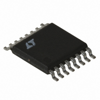
LT1976EFE Linear Technology, LT1976EFE Datasheet - Page 18

LT1976EFE
Manufacturer Part Number
LT1976EFE
Description
IC REG SW STEP DWN 1.5A 16-TSSOP
Manufacturer
Linear Technology
Type
Step-Down (Buck)r
Datasheet
1.LT1976IFEPBF.pdf
(28 pages)
Specifications of LT1976EFE
Internal Switch(s)
Yes
Synchronous Rectifier
No
Number Of Outputs
1
Voltage - Output
1.2 ~ 54 V
Current - Output
1.5A
Frequency - Switching
200kHz
Voltage - Input
3.3 ~ 60 V
Operating Temperature
-40°C ~ 125°C
Mounting Type
Surface Mount
Package / Case
16-TSSOP Exposed Pad, 16-eTSSOP, 16-HTSSOP
Lead Free Status / RoHS Status
Contains lead / RoHS non-compliant
Power - Output
-
Available stocks
Company
Part Number
Manufacturer
Quantity
Price
Part Number:
LT1976EFE
Manufacturer:
LINEAR/凌特
Quantity:
20 000
Company:
Part Number:
LT1976EFE#PBF
Manufacturer:
IR
Quantity:
120
Part Number:
LT1976EFE#PBF
Manufacturer:
LINEAR/凌特
Quantity:
20 000
Company:
Part Number:
LT1976EFE#TRPBF
Manufacturer:
LT
Quantity:
1 560
Part Number:
LT1976EFE#TRPBF
Manufacturer:
LTNEAR
Quantity:
20 000
LT1976/LT1976B
APPLICATIO S I FOR ATIO
Burst Mode OPERATION (LT1976 ONLY)
To enhance efficiency at light loads, the LT1976 automati-
cally switches to Burst Mode operation which keeps the
output capacitor charged to the proper voltage while mini-
mizing the input quiescent current. During Burst Mode
operation, the LT1976 delivers short bursts of current to
the output capacitor followed by sleep periods where the
output power is delivered to the load by the output capaci-
tor. In addition, V
duced to typically 45μA and 125μA respectively during the
sleep time. As the load current decreases towards a no
load condition, the percentage of time that the LT1976
operates in sleep mode increases and the average input
current is greatly reduced resulting in higher efficiency.
The minimum average input current depends on the V
V
network and Schottky diode leakage. It can be approxi-
mated by the following equation:
where
18
OUT
I
V
V
I
I
I
η = low current efficiency (non Burst Mode operation)
I
IN AVG
VINS
BIASS
FB
S
OUT
IN
0.5V/DIV
(
= catch diode reverse leakage at V
ratio, V
= feedback network current
= input voltage
V
= input pin current in sleep mode
OUT
= output voltage
= BIAS pin current in sleep mode
)
≅
C
I
V
LOAD
OUT
IN
C
I
C
= 12V
VINS
SS
= 47μF
frequency compensation, feedback divider
= 200mA
= GND
C
IN
SS
+
U
Figure 4. V
= 0.1μF
and BIAS quiescent currents are re-
I
SHDN
TIME (1ms/DIV)
U
+
⎛
⎜
⎝
OUT
V
V
OUT
IN
C
dV/dt
SS
W
= 0.1μF
⎞
⎟
⎠
(
I
BIASS
OUT
1976 F04
( )
+
η
I
U
FB
+
I
S
IN
)
to
Example: For V
During the sleep portion of the Burst Mode cycle, the V
pin voltage is held just below the level needed for normal
operation to improve transient response. See the Typical
Performance Characteristics section for burst and tran-
sient response waveforms.
If a no load condition can be anticipated, the supply current
can be further reduced by cycling the SHDN pin at a rate
higher than the natural no load burst frequency. Figure 6
shows Burst Mode operation with the SHDN pin. V
burst ripple is maintained while the average supply current
I
IN AVG
(
500mA/DIV
50mV/DIV
2V/DIV
V
)
V
SHDN
I
OUT
=
=
SW
45
150
125
100
45
75
50
25
Figure 6. Burst Mode with Shutdown Pin
V
V
I
Q
0
IN
OUT
μ + μ +
= 15μA
μ + μ +
0
= 12V
A
A
= 3.3V
OUT
10
5
5
= 3.3V, V
A
A
Figure 5. I
INPUT VOLTAGE (V)
20
TIME (50ms/DIV)
⎛
⎝ ⎜
47
3 3
12
μ =
.
30
A
IN
⎞
⎠ ⎟
Q
(
= 12V
125
vs V
97
40
V
IN
μ +
μ
OUT
T
A
A
A
50
= 25°C
= 3.3V
1976 F05
12 5
( )
0 8
1976 G16
60
.
.
μ +
A
0. .
5
1976bfg
μ
OUT
A
C
)


