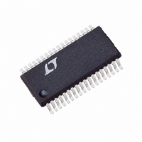
LTC1709EG#TRPBF Linear Technology, LTC1709EG#TRPBF Datasheet - Page 21

LTC1709EG#TRPBF
Manufacturer Part Number
LTC1709EG#TRPBF
Description
IC SW REG STEP-DOWN SYNC 36-SSOP
Manufacturer
Linear Technology
Type
Step-Down (Buck)r
Datasheet
1.LTC1709EG.pdf
(28 pages)
Specifications of LTC1709EG#TRPBF
Internal Switch(s)
No
Synchronous Rectifier
Yes
Number Of Outputs
2
Voltage - Output
1.3 ~ 3.5 V
Current - Output
3A
Voltage - Input
4 ~ 36 V
Operating Temperature
-40°C ~ 85°C
Mounting Type
Surface Mount
Package / Case
36-SSOP
Lead Free Status / RoHS Status
Lead free / RoHS Compliant
Power - Output
-
Frequency - Switching
-
Available stocks
Company
Part Number
Manufacturer
Quantity
Price
APPLICATIO S I FOR ATIO
and output power level. The combined effects of increas-
ingly lower output voltages and higher currents required
by high performance digital systems is not doubling but
quadrupling the importance of loss terms in the switching
regulator system!
2) Transition losses apply only to the topside MOSFET(s),
and are significant only when operating at high input
voltages (typically 12V or greater). Transition losses can
be estimated from:
3) INTV
control currents. The MOSFET driver current results from
switching the gate capacitance of the power MOSFETs.
Each time a MOSFET gate is switched from low to high to
low again, a packet of charge dQ moves from INTV
ground. The resulting dQ/dt is a current out of INTV
is typically much larger than the control circuit current. In
continuous mode, I
are the gate charges of the topside and bottom side
MOSFETs.
Supplying INTV
from an output-derived source will scale the V
required for the driver and control circuits by the ratio
(Duty Factor)/(Efficiency). For example, in a 20V to 5V
application, 10mA of INTV
mately 3mA of V
loss from 10% or more (if the driver was powered directly
from V
4) The V
DC supply current given in the Electrical Characteristics
table, which excludes MOSFET driver and control cur-
rents; the second is the current drawn from the differential
amplifier output. V
(<0.1%) loss.
Other “hidden” losses such as copper trace and internal
battery resistances can account for an additional 5% to
10% efficiency degradation in portable systems. It is very
important to include these “system” level losses in the
design of a system. The internal battery and input fuse
resistance losses can be minimized by making sure that
C
switching frequency. A 50W supply will typically require a
IN
Transition Loss = (1.7) V
has adequate charge storage and a very low ESR at the
IN
CC
) to only a few percent.
IN
current is the sum of the MOSFET driver and
current has two components: the first is the
CC
IN
power through the EXTV
current. This reduces the mid-current
IN
U
GATECHG
current typically results in a small
U
CC
IN
= (Q
2
current results in approxi-
I
O(MAX)
T
+ Q
W
B
), where Q
C
RSS
CC
f
switch input
U
IN
T
current
and Q
CC
CC
that
to
B
minimum of 200 F to 300 F of output capacitance having
a maximum of 10m
2-phase architecture typically halves the input and output
capacitance requirement over competing solutions. Other
losses including Schottky conduction losses during dead-
time and inductor core losses generally account for less
than 2% total additional loss.
Checking Transient Response
The regulator loop response can be checked by looking at
the load transient response. Switching regulators take
several cycles to respond to a step in DC (resistive) load
current. When a load step occurs, V
amount equal to I
series resistance of C
or discharge C
that forces the regulator to adapt to the current change and
return V
time V
ringing, which would indicate a stability problem. The
availability of the I
control loop behavior but also provides a DC coupled and
AC filtered closed loop response test point. The DC step,
rise time, and settling at this test point truly reflects the
closed loop response. Assuming a predominantly second
order system, phase margin and/or damping factor can be
estimated using the percentage of overshoot seen at this
pin. The bandwidth can also be estimated by examining
the rise time at the pin. The I
shown in the Figure 1 circuit will provide an adequate
starting point for most applications.
The I
loop compensation. The values can be modified slightly
(from 0.2 to 5 times their suggested values) to optimize
transient response once the final PC layout is done and the
particular output capacitor type and value have been
determined. The output capacitors need to be decided
upon because the various types and values determine the
loop gain and phase. An output current pulse of 20% to
80% of full-load current having a rise time of <2 s will
produce output voltage and I
give a sense of the overall loop stability without breaking
the feedback loop. The initial output voltage step resulting
from the step change in output current may not be within
TH
OUT
OUT
series R
can be monitored for excessive overshoot or
to its steady-state value. During this recovery
OUT
C
-C
TH
LOAD
generating the feedback error signal
C
OUT
pin not only allows optimization of
filter sets the dominant pole-zero
to 20m
(ESR), where ESR is the effective
• ( I
LOAD
TH
TH
pin waveforms that will
of ESR. The LTC1709
) also begins to charge
external components
OUT
LTC1709
shifts by an
21


