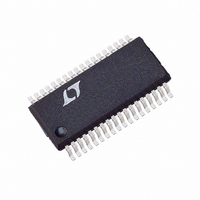
LTC1709EG#TRPBF Linear Technology, LTC1709EG#TRPBF Datasheet - Page 7

LTC1709EG#TRPBF
Manufacturer Part Number
LTC1709EG#TRPBF
Description
IC SW REG STEP-DOWN SYNC 36-SSOP
Manufacturer
Linear Technology
Type
Step-Down (Buck)r
Datasheet
1.LTC1709EG.pdf
(28 pages)
Specifications of LTC1709EG#TRPBF
Internal Switch(s)
No
Synchronous Rectifier
Yes
Number Of Outputs
2
Voltage - Output
1.3 ~ 3.5 V
Current - Output
3A
Voltage - Input
4 ~ 36 V
Operating Temperature
-40°C ~ 85°C
Mounting Type
Surface Mount
Package / Case
36-SSOP
Lead Free Status / RoHS Status
Lead free / RoHS Compliant
Power - Output
-
Frequency - Switching
-
Available stocks
Company
Part Number
Manufacturer
Quantity
Price
PI FU CTIO S
RUN/SS (Pin 1): Combination of Soft-Start, Run Control
Input and Short-Circuit Detection Timer. A capacitor to
ground at this pin sets the ramp time to full current output.
Forcing this pin below 0.8V causes the IC to shut down all
internal circuitry. All functions are disabled in shutdown.
SENSE 1
Differential Current Comparator. The I
built-in offsets between SENSE
conjunction with R
SENSE 1
Differential Current Comparators.
EAIN (Pin 4): Input to the Error Amplifier that compares
the feedback voltage to the internal 0.8V reference voltage.
This pin is normally connected to a resistive divider from
the output of the differential amplifier (DIFFOUT).
PLLFLTR (Pin 5): The Phase-Locked Loop’s Low Pass
Filter is tied to this pin. Alternatively, this pin can be driven
with an AC or DC voltage source to vary the frequency of
the internal oscillator.
PLLIN (Pin 6): External Synchronization Input to Phase
Detector. This pin is internally terminated to SGND with
50k . The phase-locked loop will force the rising top gate
signal of controller 1 to be synchronized with the rising
edge of the PLLIN signal.
TYPICAL PERFOR A CE CHARACTERISTICS
U
350
300
200
150
100
250
50
0
– 50
Oscillator Frequency
vs Temperature
+
–
– 25
, SENSE 2
, SENSE 2
U
0
TEMPERATURE ( C)
V
SENSE
25
FREQSET
V
V
FREQSET
FREQSET
+
–
U
(Pins 2,14): The (+) Input to Each
(Pins 3, 13): The (–) Input to the
50
= OPEN
set the current trip threshold.
= 5V
= 0V
75
W
100
–
1709 G23
U
and SENSE
125
TH
pin voltage and
3.50
3.45
3.20
3.40
3.35
3.30
3.25
–50
Undervoltage Lockout
vs Temperature
+
pins in
–25
0
TEMPERATURE ( C)
25
NC (Pins 7, 36): Do not connect.
I
tor Compensation Point. Both current comparator’s thresh-
olds increase with this control voltage. The normal voltage
range of this pin is from 0V to 2.4V
SGND (Pin 9): Signal Ground, common to both control-
lers. Route separately to the PGND pin.
V
provides true remote output voltage sensing. This pin
normally drives an external resistive divider that sets the
output voltage.
V
fier. Internal precision resistors capable of being elec-
tronically switched in or out can configure it as a differen-
tial amplifier or an uncommitted Op Amp.
ATTENOUT (Pin 15): Voltage Feedback Signal Resistively
Divided According to the VID Programming Code.
ATTENIN (Pin 16): The Input to the VID Controlled Resis-
tive Divider.
VID0–VID4 (Pins 17,18, 19, 20, 21): VID Control Logic
Input Pins.
V
TH
DIFFOUT
OS
BIAS
50
(Pin 8): Error Amplifier Output and Switching Regula-
–
, V
(Pin 22): Supply Pin for the VID Control Circuit.
75
OS
(Pin 10): Output of a Differential Amplifier that
+
100
(Pins 11, 12): Inputs to an Operational Ampli-
1709 G24
125
3.0
2.5
2.0
1.0
4.5
4.0
3.5
1.5
0.5
0
–50
V
Thresholds vs Temperature
RUN/SS
–25
Shutdown Latch
0
TEMPERATURE ( C)
THRESHOLD
LATCHOFF
25
LTC1709
LATCH ARMING
50
75
100
1709 G25
7
125


