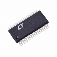
LTC1709EG#TRPBF Linear Technology, LTC1709EG#TRPBF Datasheet - Page 23

LTC1709EG#TRPBF
Manufacturer Part Number
LTC1709EG#TRPBF
Description
IC SW REG STEP-DOWN SYNC 36-SSOP
Manufacturer
Linear Technology
Type
Step-Down (Buck)r
Datasheet
1.LTC1709EG.pdf
(28 pages)
Specifications of LTC1709EG#TRPBF
Internal Switch(s)
No
Synchronous Rectifier
Yes
Number Of Outputs
2
Voltage - Output
1.3 ~ 3.5 V
Current - Output
3A
Voltage - Input
4 ~ 36 V
Operating Temperature
-40°C ~ 85°C
Mounting Type
Surface Mount
Package / Case
36-SSOP
Lead Free Status / RoHS Status
Lead free / RoHS Compliant
Power - Output
-
Frequency - Switching
-
Available stocks
Company
Part Number
Manufacturer
Quantity
Price
APPLICATIO S I FOR ATIO
The power dissipation on the topside MOSFET can be
easily estimated. Using a Siliconix Si4420DY for example;
R
voltage with T
temperature:
The worst-case power disipated by the synchronous
MOSFET under normal operating conditions at elevated
ambient temperature and estimated 50 C junction tem-
perature rise is:
A short-circuit to ground will result in a folded back current
of about:
The worst-case power disipated by the synchronous
MOSFET under short-circuit conditions at elevated ambi-
ent temperature and estimated 50 C junction temperature
rise is:
which is less than half of the normal, full-load conditions.
Incidentally, since the load no longer dissipates power in
the shorted condition, total system power dissipation is
decreased by over 99%.
DS(ON)
P
P
I
P
SC
MAIN
SYNC
SYNC
= 0.013 , C
0 004
25
.
0 013
1 29
1 8
5 5
630
300
5 5
5 5
.
mV
.
.
.
.
.
j
(estimated) = 110 C at an elevated ambient
V
V
V
V
5 5
5 5
mW
kHz
W
.
.
10 1
V
V
U
1 8
1 8
2
1
.
.
2
1 7 5 5
RSS
V
0 65
V
.
200
.
7
10
U
1 5
= 300pF. At maximum input
A
ns
.
W
0 005 110
.
A
.
V
2
5 5
2
H
1 48 0 013
2
.
.
1 48 0 013
10
V
.
W
A
.
300
C
7
.
A
pF
25
U
C
The duty factor for this application is:
Using Figure 4, the RMS ripple current will be:
An input capacitor(s) with a 4.6A
is required.
The output capacitor ripple current is calculated by using
the inductor ripple already calculated for each inductor
and multiplying by the factor obtained from Figure 3 along
with the calculated duty factor. The output ripple in con-
tinuous mode will be highest at the maximum input
voltage since the duty factor is < 50%. The maximum
output current ripple is:
PC Board Layout Checklist
When laying out the printed circuit board, the following
checklist should be used to ensure proper operation of the
LTC1709. These items are also illustrated graphically in
the layout diagram of Figure 11. Check the following in
your layout:
1) Are the signal and power grounds segregated? The
LTC1709 signal ground pin should return to the (–) plate
of C
sources of the bottom N-channel MOSFETs, anodes of the
Schottky diodes, and (–) plates of C
as short lead lengths as possible.
2) Does the LTC1709 V
load? Does the LTC1709 V
return?
I
DF
V
INRMS
. .
OUTRIPPLE
OUT
I
I
COUT
COUTMAX
separately. The power ground returns to the
V
V
= (20A)(0.23) = 4.6A
IN
O
V
OUT
fL
1 8
5
.
1 2
20
V
300
.
V
m
0 3
A
.
RMS
kHz
0 36
1 8
OS
1 2
.
at
.
.
+
V
33
1 5
A
OS
pin connect to the point of
.
RMS
% . .
–
RMS
RMS
pin connect to the load
D F
H
IN
0 3
ripple current rating
.
, which should have
24
LTC1709
mV
RMS
23


