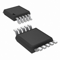
LM3481MMX/NOPB National Semiconductor, LM3481MMX/NOPB Datasheet - Page 9

LM3481MMX/NOPB
Manufacturer Part Number
LM3481MMX/NOPB
Description
IC CTLR N-CH LOW SIDE HE 10MSOP
Manufacturer
National Semiconductor
Type
Step-Up (Boost), Flyback, Sepicr
Datasheet
1.LM3481MMNOPB.pdf
(22 pages)
Specifications of LM3481MMX/NOPB
Internal Switch(s)
No
Synchronous Rectifier
No
Number Of Outputs
1
Voltage - Output
Adjustable
Current - Output
1A
Frequency - Switching
100kHz ~ 1MHz
Voltage - Input
2.97 ~ 48 V
Operating Temperature
-40°C ~ 125°C
Mounting Type
Surface Mount
Package / Case
10-MSOP, Micro10™, 10-uMAX, 10-uSOP
For Use With
LM3481EVAL - BOARD EVAL FOR LM3481
Lead Free Status / RoHS Status
Lead free / RoHS Compliant
Power - Output
-
Other names
LM3481MMX
Available stocks
Company
Part Number
Manufacturer
Quantity
Price
Company:
Part Number:
LM3481MMX/NOPB
Manufacturer:
TI
Quantity:
12 000
OVER VOLTAGE PROTECTION
The LM3481 has over voltage protection (OVP) for the output
voltage. OVP is sensed at the feedback pin (FB). If at anytime
the voltage at the feedback pin rises to V
triggered. See the electrical characteristics section for limits
on V
OVP will cause the drive pin (DR) to go low, forcing the power
MOSFET off. With the MOSFET off, the output voltage will
drop. The LM3481 will begin switching again when the feed-
back voltage reaches V
trical characteristics section for limits on V
The internal bias of the LM3481 comes from either the internal
bias voltage generator as shown in the block diagram or di-
rectly from the voltage at the VIN pin. At input voltages lower
than 6V the internal IC bias is the input voltage and at voltages
above 6V the internal bias voltage generator of the LM3481
provides the bias.
SLOPE COMPENSATION RAMP
The LM3481 uses a current mode control scheme. The main
advantages of current mode control are inherent cycle-by-cy-
cle current limit for the switch and simpler control loop char-
acteristics. It is easy to parallel power stages using current
mode control since current sharing is automatic. However
there is a natural instability that will occur for duty cycles, D,
greater than 50% if additional slope compensation is not ad-
dressed as described below.
The current mode control scheme samples the inductor cur-
rent, I
nally generated control signal, V
R
current, I
I
The rising and falling slopes, M
V
L
samp
SEN
such that:
FB
, as shown in
L
are also proportional to the inductor current rising and
, and compares the sampled signal, V
and V
L
, to the voltage signal, V
OVP
.
Figure
V
samp
FB
+ (V
5, converts the sampled inductor
= I
OVP
L
c
x R
. The current sense resistor,
1
samp
- V
and −M
SEN
FIGURE 1. Basic Operation of the PWM comparator
OVP(HYS)
, that is proportional to
FB
OVP(HYS)
2
+ V
respectively, of
). See the elec-
samp
OVP
, to a inter-
.
, OVP is
9
falling slopes, M
inductor slope during the switch on-time and −M
ductor slope during the switch off-time and are related to M
and −M
For the boost topology:
Current mode control has an inherent instability for duty cy-
cles greater than 50%, as shown in
signal slope, M
the load current causes the sampled signal to increase by
ΔV
of the first switching cycle is :
From the above equation, when D > 0.5, ΔV
greater than ΔV
vergent. So a very small perturbation in the load will cause
the disturbance to increase. To ensure that the perturbed sig-
nal converges we must maintain:
samp0
2
. The effect of this load change, ΔV
by:
−M
C
M
, equals zero. In
samp0
on
2
2
−M
= [(V
and −M
= [(V
M
−M
. In other words, the disturbance is di-
M
off
1
= [V
1
2
M
OUT
= (V
IN
= M
= −M
on
− V
off
IN
− V
= V
IN
on
respectively. Where M
/ L] x R
OUT
off
− V
IN
x R
IN
Figure
) / L] x R
x R
) / L] x R
/ L
OUT
Figure
SEN
SEN
SEN
) / L
2, a small increase in
2, where the control
SEN
SEN
samp1
samp1
www.national.com
20136507
, at the end
off
is the in-
on
will be
is the
1


