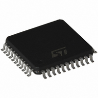
L6710 STMicroelectronics, L6710 Datasheet - Page 26

L6710
Manufacturer Part Number
L6710
Description
IC CTRLR 6BIT 2PH PROGR 44-TQFP
Manufacturer
STMicroelectronics
Type
Step-Down (Buck)r
Datasheet
1.L6710.pdf
(34 pages)
Specifications of L6710
Internal Switch(s)
No
Synchronous Rectifier
Yes
Number Of Outputs
2
Voltage - Output
0.84 ~ 1.6 V
Current - Output
2A
Frequency - Switching
150kHz
Voltage - Input
12V
Operating Temperature
0°C ~ 125°C
Mounting Type
Surface Mount
Package / Case
44-TQFP, 44-VQFP
Power - Output
2.5W
Product
Half-Bridge Drivers
Supply Current
12.5 mA
Mounting Style
SMD/SMT
Lead Free Status / RoHS Status
Lead free / RoHS Compliant
Available stocks
Company
Part Number
Manufacturer
Quantity
Price
Company:
Part Number:
L671000
Manufacturer:
PHI
Quantity:
1 870
Part Number:
L671000
Manufacturer:
OKI
Quantity:
20 000
L6710
Since the generated noise is mainly due to the switching activity of the VRM, noise emissions depend on
how fast the current switch. To reduce noise emission levels, it is also possible, in addition to the previous
guidelines, to reduce the current slope and then to increase the switching times: this will cause, as a con-
sequence of the higher switching time, an increase in switching losses that must be considered in the ther-
mal design of the system.
Figure 19. - Layout Suggestions (not in scale).
Application Board Description
The application board shows the operation of the device in a dual phase application. This evaluation board
allows output voltage adjustability (0.8375V - 1.6000V) through the switches S0-S4 and high output cur-
rent capability.
The board has been laid out with the possibility to use up to two D
in order to give maximum flexibility in the mosfet choice.
The four layers demo board's copper thickness is of 70 µ m in order to minimize conduction losses consid-
ering the high current that the circuit is able to deliver.
Demo board schematic circuit is reported in Figure 20.
Several jumpers allow setting different configurations for the device: JP3, JP4 and JP5 allow configuring
the remote buffer as desired. Simply shorting JP4 and JP5 the remote buffer is enabled and it senses the
output voltage on-board; to implement a real remote sense, leave these jumpers open and connect the
FBG and FBR connectors on the demo board to the remote load.
To avoid using the remote buffer, simply short all the jumpers JP3, JP4 and JP5. Local sense through the
R7 is used for the regulation.
The input can be configured in different ways using the jumpers JP1, JP2 and JP6; these jumpers control
also the mosfet driver supply voltage. Anyway, power conversion starts from VIN and the device is sup-
plied from V
26/34
CC
PHASE PLANE
NTC FOR
THERMAL
COMPENSATION
OUTPUT
POWER PLANE
(See Figure 21).
ATX 12 CONNECTOR
INPUT POWER PLANE
2
PACK mosfets for the low side switch
INPUT CAPS
PHASE PLANE
SAFELY FAR
HIGH SPEED
DATA BUS
OUTPUT BULK
CAPACITORS
DECOUPLING
CAPACITORS
CERAMIC


