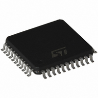
L6710 STMicroelectronics, L6710 Datasheet - Page 27

L6710
Manufacturer Part Number
L6710
Description
IC CTRLR 6BIT 2PH PROGR 44-TQFP
Manufacturer
STMicroelectronics
Type
Step-Down (Buck)r
Datasheet
1.L6710.pdf
(34 pages)
Specifications of L6710
Internal Switch(s)
No
Synchronous Rectifier
Yes
Number Of Outputs
2
Voltage - Output
0.84 ~ 1.6 V
Current - Output
2A
Frequency - Switching
150kHz
Voltage - Input
12V
Operating Temperature
0°C ~ 125°C
Mounting Type
Surface Mount
Package / Case
44-TQFP, 44-VQFP
Power - Output
2.5W
Product
Half-Bridge Drivers
Supply Current
12.5 mA
Mounting Style
SMD/SMT
Lead Free Status / RoHS Status
Lead free / RoHS Compliant
Available stocks
Company
Part Number
Manufacturer
Quantity
Price
Company:
Part Number:
L671000
Manufacturer:
PHI
Quantity:
1 870
Part Number:
L671000
Manufacturer:
OKI
Quantity:
20 000
Figure 20. Demo Board Schematic
Figure 21. Power supply configuration
Two main configurations can be distinguished: Single Supply (V
(V
Some examples are reported in the following Figures 22 and 23.
GNDin
GNDcc
CC
– Single Supply: In this case JP6 has to be completely shorted. The device is supplied with the same
– Double Supply: In this case VCC supply directly the controller (12V) while VIN supplies the HS drains
Vcc
Vin
L6710 EVALUATION BOARD REV.1
=12V V
rail that is used for the conversion. With an additional zener diode DZ1 a lower voltage can be derived
to supply the mosfets driver if Logic level mosfet are used. In this case JP1 must be left open so that
the HS driver is supplied with V
VIN or to the right to use V
be shorted and JP2 can be freely shorted in one of the two positions.
for the power conversion. This last one can start indifferently from the 5V bus (Typ.) or from other
buses allowing maximum flexibility in the power conversion. Supply for the mosfet driver can be pro-
grammed through the jumpers JP1, JP2 and JP6 as previously illustrated. JP6 selects now VCC or
V
IN
depending on the requirements.
JP6
IN
OUTEN
S4
S3
S2
S1
S0
S5
=5V or different).
L1
Vcc pin
C5
GNDin
GNDcc
To
Vcc
DZ1
JP1
Vin
C4
D1
Q1a
R21
D4
Q2
Q1
R16
R2
JP6
JP2
C8
IN
R15
R18
R13
R6
R5
-V
C25
DZ1
UGATE1
PGNDS
PHASE1
LGATE1
OUTEN
VCCDR
BOOT1
SGND
ISEN1
To
OSC
VID5
VID4
VID3
VID2
VID1
VID0
IN
-V
to supply the LS driver through VCCDR pin. Otherwise, JP1 must
6, 7
19
29
28
27
26
25
24
14
22
41
43
42
40
REF_OUT
3
DZ1
L6710
DZ1
JP1
12
U1
through BOOTx and JP2 must be shorted to the left to use
FBR
17
18
JP2
31
35
36
38
21
20
39
30
13
FBG
5
9
8
VCC
BOOT2
UGATE2
PHASE2
LGATE2
ISEN2
PGNDS
PGND
PGOOD
FB
COMP
VSEN
C26
R17
R12
R14
R3
R4
To BOOTx (HS Driver Supply)
To Vcc pin
To HS Drains (Power Input)
C7
To VCCDR pin (LS Driver Supply)
R11
C28
R10
C2
R8
Q4
Q3
R7a
R7
D3
C1
D2
Q3a
C3
CC
JP7
JP8
R9
=V
C6
L2
R22
IN
=12V) and Double Supply
NTC1
Vcc pin
To
C9,C10
C15,
C24
JP3
C11..C14
R1
JP4
R19
R20
JP5
L6710
VoutCORE
GNDCORE
PGOOD
FBG
FBR
27/34


