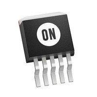
MC33167D2T ON Semiconductor, MC33167D2T Datasheet - Page 3

MC33167D2T
Manufacturer Part Number
MC33167D2T
Description
IC REG SWITCH INVERT 5A D2PAK-5
Manufacturer
ON Semiconductor
Type
Step-Down (Buck), Step-Up (Boost), Invertingr
Datasheet
1.MC33167TG.pdf
(20 pages)
Specifications of MC33167D2T
Internal Switch(s)
Yes
Synchronous Rectifier
No
Number Of Outputs
1
Voltage - Output
5 ~ 40 V
Current - Output
5A
Frequency - Switching
72kHz
Voltage - Input
7.5 ~ 40 V
Operating Temperature
-40°C ~ 85°C
Mounting Type
Surface Mount
Package / Case
D²Pak, TO-263 (5 leads + tab)
Mounting Style
SMD/SMT
Lead Free Status / RoHS Status
Contains lead / RoHS non-compliant
Power - Output
-
Lead Free Status / Rohs Status
Lead free / RoHS Compliant
Available stocks
Company
Part Number
Manufacturer
Quantity
Price
Company:
Part Number:
MC33167D2T
Manufacturer:
ON
Quantity:
347
Company:
Part Number:
MC33167D2T
Manufacturer:
MOT
Quantity:
5 510
Company:
Part Number:
MC33167D2TC
Manufacturer:
TI
Quantity:
5 510
4. Low duty cycle pulse techniques are used during test to maintain junction temperature as close to ambient as possible.
5. T
ELECTRICAL CHARACTERISTICS
temperature range that applies (Notes 4, 5), unless otherwise noted.)
OSCILLATOR
ERROR AMPLIFIER
PWM COMPARATOR
SWITCH OUTPUT
UNDERVOLTAGE LOCKOUT
TOTAL DEVICE
Frequency (V
Voltage Feedback Input Threshold
Line Regulation (V
Input Bias Current (V
Power Supply Rejection Ratio (V
Output Voltage Swing
Duty Cycle (V
Output Voltage Source Saturation (V
Off−State Leakage (V
Current Limit Threshold (V
Switching Times (V
Startup Threshold (V
Hysteresis (V
Power Supply Current (T
Output Voltage Rise Time
Output Voltage Fall Time
Standby (V
Operating (V
low
= 0°C for MC34167
= − 40°C for MC33167
CC
CC
CC
CC
CC
= 7.5 V to 40 V)
= 12 V, V
= 20 V)
Decreasing, T
= 40 V, Pin 1 = GND for maximum duty cycle)
CC
CC
FB
CC
= 7.5 V to 40 V, T
CC
= 40 V, I
= V
High State (I
Low State (I
A
Increasing, T
Characteristic
= 40 V, Pin 2 = GND)
Comp
CC
= +25°C )
FB(th)
= 7.5 V)
pk
A
< 0.15 V)
CC
= +25°C)
+ 0.15 V)
= 5.0 A, L = 225 mH, T
= 10 V to 20 V, f = 120 Hz)
Sink
Source
CC
A
Maximum (V
Minimum (V
A
= +25°C)
= 7.5 V, I
= 0.4 mA, V
= +25°C)
(V
T
high
CC
= 75 mA, V
= 12 V, for typical values T
= + 70°C for MC34167
= + 85°C for MC33167
T
T
T
T
A
A
A
A
Source
Comp
FB
= +25°C
= T
=+ 25°C
= T
MC34167, MC33167
FB
= 0 V)
FB
low
low
= 5.5 V)
= 1.9 V)
= 5.0 A)
A
http://onsemi.com
= 4.5 V)
= +25°C)
to T
to T
high
high
3
V
I
V
Symbol
DC
DC
pk(switch)
Reg
V
PSRR
I
th(UVLO)
H(UVLO)
A
f
sw(off)
V
V
V
OSC
FB(th)
I
I
CC
OH
(max)
t
= +25°C, for min/max values T
IB
OL
(min)
sat
t
r
f
line
4.95
4.85
Min
4.2
5.5
5.5
0.6
65
62
60
92
−
−
−
0
−
−
−
−
−
−
(V
CC
5.05
0.03
0.15
Typ
100
4.9
1.6
6.5
5.9
0.9
72
80
95
50
36
40
−
−
0
0
−1.5)
A
is the operating ambient
(V
CC
0.078
Max
5.15
5.20
100
100
200
100
100
1.0
1.9
8.0
6.3
1.2
79
81
60
−
−
0
−1.8)
Unit
%/V
kHz
mA
dB
mA
mA
mA
ns
%
V
V
V
A
V
V


