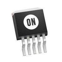
MC33167D2T ON Semiconductor, MC33167D2T Datasheet - Page 7

MC33167D2T
Manufacturer Part Number
MC33167D2T
Description
IC REG SWITCH INVERT 5A D2PAK-5
Manufacturer
ON Semiconductor
Type
Step-Down (Buck), Step-Up (Boost), Invertingr
Datasheet
1.MC33167TG.pdf
(20 pages)
Specifications of MC33167D2T
Internal Switch(s)
Yes
Synchronous Rectifier
No
Number Of Outputs
1
Voltage - Output
5 ~ 40 V
Current - Output
5A
Frequency - Switching
72kHz
Voltage - Input
7.5 ~ 40 V
Operating Temperature
-40°C ~ 85°C
Mounting Type
Surface Mount
Package / Case
D²Pak, TO-263 (5 leads + tab)
Mounting Style
SMD/SMT
Lead Free Status / RoHS Status
Contains lead / RoHS non-compliant
Power - Output
-
Lead Free Status / Rohs Status
Lead free / RoHS Compliant
Available stocks
Company
Part Number
Manufacturer
Quantity
Price
Company:
Part Number:
MC33167D2T
Manufacturer:
ON
Quantity:
347
Company:
Part Number:
MC33167D2T
Manufacturer:
MOT
Quantity:
5 510
Company:
Part Number:
MC33167D2TC
Manufacturer:
TI
Quantity:
5 510
switching regulators that are optimized for dc−to−dc
converter applications. These devices operate as fixed
frequency, voltage mode regulators containing all the active
functions required to directly implement step−down and
voltage−inverting converters with a minimum number of
external components. They can also be used cost effectively
in step−up converter applications. Potential markets include
automotive, computer, industrial, and cost sensitive
consumer products. A description of each section of the
device is given below with the representative block diagram
shown in Figure 14.
Oscillator
72 kHz by capacitor C
charge to discharge ratio is controlled to yield a 95%
maximum duty cycle at the Switch Output. During the
discharge of C
pulse that holds the inverting input of the AND gate high,
disabling the output switch transistor. The nominal
oscillator peak and valley thresholds are 4.1 V and 2.3 V
respectively.
Pulse Width Modulator
the oscillator ramp voltage applied to the noninverting input,
while the error amplifier output is applied into the inverting
input. Output switch conduction is initiated when C
discharged to the oscillator valley voltage. As C
a voltage that exceeds the error amplifier output, the latch
resets, terminating output transistor conduction for the
duration of the oscillator ramp−up period. This PWM/Latch
combination prevents multiple output pulses during a given
oscillator clock cycle. Figures 7 and 15 illustrate the switch
output duty cycle versus the compensation voltage.
Current Sense
limiting as a means of protecting the output switch transistor
from overstress. Each on cycle is treated as a separate
situation. Current limiting is implemented by monitoring the
output switch transistor current buildup during conduction,
and upon sensing an overcurrent condition, immediately
turning off the switch for the duration of the oscillator
ramp−up period.
internal trimmed resistor and compared against a reference
by the Current Sense comparator. When the current limit
threshold is reached, the comparator resets the PWM latch.
The current limit threshold is typically set at 6.5 A.
The MC34167, MC33167 series are monolithic power
The oscillator frequency is internally programmed to
The Pulse Width Modulator consists of a comparator with
The MC34167 series utilizes cycle−by−cycle current
The collector current is converted to a voltage by an
T
, the oscillator generates an internal blanking
T
and a trimmed current source. The
T
MC34167, MC33167
charges to
http://onsemi.com
INTRODUCTION
T
is
7
Figure 10 illustrates switch output current limit threshold
versus temperature.
Error Amplifier and Reference
inverting input and output. This amplifier features a typical
dc voltage gain of 80 dB, and a unity gain bandwidth of
600 kHz with 70 degrees of phase margin (Figure 4). The
noninverting input is biased to the internal 5.05 V reference
and is not pinned out. The reference has an accuracy of
± 2.0% at room temperature. To provide 5.0 V at the load,
the reference is programmed 50 mV above 5.0 V to
compensate for a 1.0% voltage drop in the cable and
connector from the converter output. If the converter design
requires an output voltage greater than 5.05 V, resistor R
must be added to form a divider network at the feedback
input as shown in Figures 14 and 19. The equation for
determining the output voltage with the divider network is:
stability. A simple low−pass filter is formed by connecting
a resistor (R
input, and a series resistor−capacitor (R
1 and 5. The compensation network component values
shown in each of the applications circuits were selected to
provide stability over the tested operating conditions. The
step−down converter (Figure 19) is the easiest to
compensate for stability. The step−up (Figure 21) and
voltage−inverting (Figure 23) configurations operate as
continuous conduction flyback converters, and are more
difficult to compensate. The simplest way to optimize the
compensation network is to observe the response of the
output voltage to a step load change, while adjusting R
C
for stability under four boundary conditions. These
conditions are minimum and maximum input voltages, with
minimum and maximum loads.
(Pin 5) to less than 150 mV, the internal circuitry will be
placed into a low power standby mode, reducing the
power supply current to 36 mA with a 12 V supply voltage.
Figure 11 illustrates the standby supply current versus
supply voltage.
pull−up that can be used to implement soft−start. Figure 18
shows the current source charging capacitor C
series diode. The diode disconnects C
loop when the 1.0 M resistor charges it above the operating
range of Pin 5.
F
A high gain Error Amplifier is provided with access to the
External loop compensation is required for converter
By clamping the voltage on the error amplifier output
The Error Amplifier output has a 100 mA current source
for critical damping. The final circuit should be verified
2
) from the regulated output to the inverting
V out + 5.05
R 2
R 1
) 1
SS
F
, C
from the feedback
F
) between Pins
SS
through a
F
and
1


