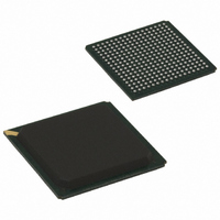
KSZ8695P Micrel Inc, KSZ8695P Datasheet - Page 25

KSZ8695P
Manufacturer Part Number
KSZ8695P
Description
IC ARM9 W/MMU PHY 10/100 289PBGA
Manufacturer
Micrel Inc
Specifications of KSZ8695P
Applications
*
Mounting Type
Surface Mount
Package / Case
289-PBGA
Operating Supply Voltage (typ)
1.8/3.3V
Operating Supply Voltage (min)
1.7/3V
Operating Supply Voltage (max)
1.9/3.6V
Operating Temp Range
0C to 70C
Operating Temperature Classification
Commercial
Mounting
Surface Mount
Pin Count
289
For Use With
576-1623 - BOARD EVALUATION KSZ8695P-MMB
Lead Free Status / RoHS Status
Lead free / RoHS Compliant
Other names
576-1509-5
KSZ8695P
KSZ8695P
Available stocks
Company
Part Number
Manufacturer
Quantity
Price
Company:
Part Number:
KSZ8695P
Manufacturer:
MICREL30
Quantity:
84
Part Number:
KSZ8695PX
Manufacturer:
MICREL
Quantity:
20 000
Signal Descriptions by Group
Clock and Reset Pins
JTAG Interface Pins
WAN Ethernet Physical Interface Pins
Note:
1. I = Input.
Micrel, Inc.
May 2006
M15
U17
G14
G15
A17
T17
F14
F15
F16
Pin
Pin
Pin
G1
G2
G3
G4
G5
E1
E2
O = Output.
O/I = Output in normal mode; input pin during reset.
CPUCLKSEL
WANFXSD
WRSTPLS
WANRXM
WANTXM
WANRXP
WANTXP
CPUCLK
RESETN
EROEN/
URTSN/
WRSTO
XCLK1/
TRSTN
XCLK2
Name
Name
Name
TMS
TDO
TCK
TDI
I/O Type
I/O Type
I/O Type
O/I
O/I
O
O
O
O
I
I
I
I
I
I
I
I
I
I
(1)
(1)
(1)
Description
External Clock In. This signal is used as the source clock for the transmit clock of
the internal MAC and PHY. The clock frequency is 25MHz ±50ppm. The XCLK1
signal is also used as the reference clock signal for the internal PLL to generate the
125MHz internal system clock.
External Clock In. Used with XCLK1 pin when another polarity of crystal is needed.
This is unused for a normal clock input.
Normal Mode: UART request to send. Active low output.
During reset: CPU clock select. Select CPU clock source. CPUCLKSEL=0 (normal
mode), the internal PLL clock output is used as the CPU clock source.
CPUCLKSEL=1 (factory reserved test signal).
KS8695P chip reset. Active low input asserted for at least 256 system clock (40ns)
cycles to reset the KS8695P. When in the reset state, all the output pins are tri-
stated and all open drain signals are floating.
Watchdog timer reset output. This signal is asserted for at least 200ms if RESETN
is asserted or when the internal watchdog timer expires.
Normal Mode: ROM/SRAM/FLASH and External I/O output enable. Active low.
When asserted, this signal controls the output enable port of the specified device.
During reset: Watchdog timer reset polarity setting. WRSTPLS=0, Active high;
WRSTPLS=1, Active low. No default.
Description
JTAG test clock.
JTAG test mode select.
JTAG test data in.
JTAG test data out.
JTAG test reset. Active low.
Description
WAN PHY transmit signal + (differential).
WAN PHY transmit signal – (differential).
WAN PHY receive signal + (differential).
WAN PHY receive signal – (differential).
WAN fiber signal detect. Signal detect input when the WAN port is operated in
100BASE-FX 100Mb fiber mode. See Application Note 10.
25
M9999-051806
KS8695P


