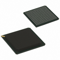
KSZ8695P Micrel Inc, KSZ8695P Datasheet - Page 31

KSZ8695P
Manufacturer Part Number
KSZ8695P
Description
IC ARM9 W/MMU PHY 10/100 289PBGA
Manufacturer
Micrel Inc
Specifications of KSZ8695P
Applications
*
Mounting Type
Surface Mount
Package / Case
289-PBGA
Operating Supply Voltage (typ)
1.8/3.3V
Operating Supply Voltage (min)
1.7/3V
Operating Supply Voltage (max)
1.9/3.6V
Operating Temp Range
0C to 70C
Operating Temperature Classification
Commercial
Mounting
Surface Mount
Pin Count
289
For Use With
576-1623 - BOARD EVALUATION KSZ8695P-MMB
Lead Free Status / RoHS Status
Lead free / RoHS Compliant
Other names
576-1509-5
KSZ8695P
KSZ8695P
Available stocks
Company
Part Number
Manufacturer
Quantity
Price
Company:
Part Number:
KSZ8695P
Manufacturer:
MICREL30
Quantity:
84
Part Number:
KSZ8695PX
Manufacturer:
MICREL
Quantity:
20 000
Advanced Memory Interface (SDRAM/ROM/FLASH/SRAM/EXTERNAL I/O) (continued)
Note:
1. I = Input.
Micrel, Inc.
May 2006
R10
U10
R11
U11
R12
U12
R13
U13
R14
U14
U15
U16
R16
R15
P10
T10
P11
T11
P12
T12
P13
T13
P14
T14
T15
T16
P16
P15
Pin
P7
R7
P8
R8
U8
P9
R9
U9
R4
P5
R5
U5
P6
R6
U6
T8
T9
T5
T6
O = Output.
I/O = Bidirectional.
SDCSN[1]
SDCSN[0]
DATA[31]
DATA[30]
DATA[29]
DATA[28]
DATA[27]
DATA[26]
DATA[25]
DATA[24]
DATA[23]
DATA[22]
DATA[21]
DATA[20]
DATA[19]
DATA[18]
DATA[17]
DATA[16]
DATA[15]
DATA[14]
DATA[13]
DATA[12]
DATA[11]
DATA[10]
SDRASN
SDCASN
SDQM[3]
SDQM[2]
SDQM[1]
SDQM[0]
RCSN[1]
RCSN[0]
ECSN[2]
ECSN[1]
ECSN[0]
EWAITN
DATA[9]
DATA[8]
DATA[7]
DATA[6]
DATA[5]
DATA[4]
DATA[3]
DATA[2]
DATA[1]
DATA[0]
SDWEN
Name
I/O Type
I/O
O
O
O
O
O
O
O
I
(1)
Description
External Data Bus. 32-Bit bi-directional data bus for data transfer. The KS8695P
also supports 8-bit and 16-bit data bus widths.
SDRAM Chip Select: Active low chip select pins for SDRAM. The KS8695P
supports up to two SDRAM banks. One SDCSN output is provided for each bank.
SDRAM Row Address Strobe: Active low. The row address strobe pin for SDRAM.
SDRAM Column Address Strobe: Active low. The column address strobe pin for
SDRAM.
SDRAM Write Enable: Active low. The write enable signal for SDRAM.
SDRAM Data Input/Output Mask: Data input/output mask signals for SDRAM. The
SDQM is sampled high and is an output mask signal for write accesses and an
output enable signal for read accesses. Input data are masked during a write cycle.
The SDQM0/1/2/3 correspond to DATA[7:0], DATA[15:8], DATA[23:16] and
DATA[31:24], respectively.
External I/O Device Chip Select: Active low. Three external I/O banks are provided
for external memory mapped I/O operations. Each I/O bank stores up to 16KB.
The ECSNx signals indicate which of the three I/O banks is selected.
External Wait: Active low. This signal is asserted when an external I/O device or a
ROM/SRAM/FLASH bank needs more access cycles than those defined in the
corresponding control register.
ROM/SRAM/FLASH Chip Select: Active low. The KS8695P can access up to two
external ROM/SRAM/FLASH memory banks. The RCSN pins can be controlled to
map the CPU addresses into physical memory banks.
31
M9999-051806
KS8695P


