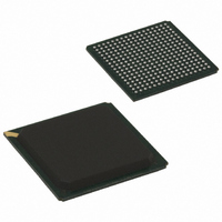
KSZ8695P Micrel Inc, KSZ8695P Datasheet - Page 28

KSZ8695P
Manufacturer Part Number
KSZ8695P
Description
IC ARM9 W/MMU PHY 10/100 289PBGA
Manufacturer
Micrel Inc
Specifications of KSZ8695P
Applications
*
Mounting Type
Surface Mount
Package / Case
289-PBGA
Operating Supply Voltage (typ)
1.8/3.3V
Operating Supply Voltage (min)
1.7/3V
Operating Supply Voltage (max)
1.9/3.6V
Operating Temp Range
0C to 70C
Operating Temperature Classification
Commercial
Mounting
Surface Mount
Pin Count
289
For Use With
576-1623 - BOARD EVALUATION KSZ8695P-MMB
Lead Free Status / RoHS Status
Lead free / RoHS Compliant
Other names
576-1509-5
KSZ8695P
KSZ8695P
Available stocks
Company
Part Number
Manufacturer
Quantity
Price
Company:
Part Number:
KSZ8695P
Manufacturer:
MICREL30
Quantity:
84
Part Number:
KSZ8695PX
Manufacturer:
MICREL
Quantity:
20 000
General Purpose I/O Pins (continued)
Micrel, Inc.
May 2006
D12
C12
D13
C13
C14
D15
B12
A12
B13
A13
B14
A14
B15
Pin
D4
C2
C3
C4
B2
B3
B4
A4
D5
B5
C5
A5
D6
B6
C6
B7
C7
A7
D8
B8
D9
A8
C9
REQ3N
REQ2N
REQ1N
GNT3N
GNT2N
GNT1N
PAD31
PAD30
PAD29
PAD28
PAD27
PAD26
PAD25
PAD24
PAD23
PAD22
PAD21
PAD20
PAD19
PAD18
PAD17
PAD16
PAD15
PAD14
PAD13
PAD12
PAD11
PAD10
Name
PCLK
PAD9
PAD8
PAD7
PAD6
PAD5
PAD4
PAD3
I/O Type
I/O
O
O
O
I
I
I
I
(1)
Description
PCI bus clock.This signal provides the timing for the PCI bus transactions. This
signal is used to drive the PCI bus interface and the internal PCI logic. All PCI bus
signals are sampled on the rising edges of the PCLK. PCLK can operate from
20MHz to 33MHz. For host mode, use PCLKOUT0 signal to drive this input. In
guest mode, use the system PCI clock to drive this input.
PCI bus grant 3. Active low. In host bridge mode, this is an output signal from the
internal PCI arbiter to grant PCI bus access to the device connected to REQ3N. In
guest bridge mode, this signal is reserved.
PCI bus grant 2. Active low. In host bridge mode, this is an output signal from the
internal PCI arbiter to grant PCI bus access to the device connected to REQ2N. In
guest bridge mode, this signal is reserved.
PCI bus grant 1. Active low. In host bridge mode, this is an output signal from the
internal PCI arbiter to grant PCI bus access to the device connected to REQ1N. In
guest bridge mode, this signal is an output to indicate that the KS8695P is
requesting to access the PCI bus as a PCI master. In guest bridge mode, this is
basically the KS8695P’s request output.
PCI bus request 3. Active low. In host bridge mode, this is an input signal from the
external PCI device to request PCI bus access. In guest bridge mode, this signal is
reserved.
PCI bus request 2. Active low. In host bridge mode, this is an input signal from the
external PCI device to request PCI bus access.In guest bridge mode, this signal is
reserved.
PCI bus request 1. Active low. In host bridge mode, this is an input signal from the
external PCI device to request PCI bus access. In guest bridge mode, this is an
input signal from an external PCI bus arbiter granting access to the bus. In guest
bridge, this is basically the KS8695P's grant input.
32-Bit PCI address and data. PCI bus transactions consist of an address phase
followed by one or more data phases. Address and data signals are multiplexed on
the same pins. For a PCI write transaction, the source of the data is the KS8695P.
For a PCI read transaction, the data source is the target. The KS8695P supports
both read and write burst transactions. In the case of a read transaction, a special
data turn around cycle is needed between the address phase and the data
phase(s).
28
M9999-051806
KS8695P


