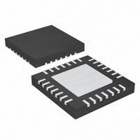
DS1865T+ Maxim Integrated Products, DS1865T+ Datasheet - Page 11

DS1865T+
Manufacturer Part Number
DS1865T+
Description
IC PON TRIPLEXER CTRLR 28TQFN-EP
Manufacturer
Maxim Integrated Products
Datasheet
1.DS1865TTR.pdf
(66 pages)
Specifications of DS1865T+
Applications
*
Mounting Type
Surface Mount
Package / Case
28-TQFN Exposed Pad
Lead Free Status / RoHS Status
Lead free / RoHS Compliant
The APC loop’s feedback is the monitor diode (BMD)
current, which is converted to a voltage using an exter-
nal resistor. The feedback voltage is compared to an 8-
bit scaleable voltage reference that determines the
APC set point of the system. Scaling of the reference
voltage accommodates the wide range in photodiode
sensitivities. This allows the application to take full
advantage of the APC reference’s resolution.
The DS1865 has an LUT to allow the APC set point to
change as a function of temperature to compensate for
tracking error (TE). The TE LUT (Table 05h) has 36
entries that determine the APC setting in 4°C windows
between -40°C to +100°C. Ranging of the APC DAC is
possible by programming a single byte in Table 02h.
The MOD output is an 8-bit scaleable voltage output that
interfaces with the MAX3643’s VMSET input. An external
resistor to ground from the MAX3643’s MODSET pin sets
the maximum current the voltage at VMSET input can
produce for a given output range. This resistor value
should be chosen to produce the maximum modulation
current the laser type requires over temperature. Then
the MOD output’s scaling is used to calibrate the full-
scale (FS) modulation output to a particular laser’s
requirements. This allows the application to take full
advantage of the MOD output’s resolution. The modula-
tion LUT can be programmed in 2°C increments over the
-40°C to +102°C range.
Ranging of the MOD DAC is possible by programming
a single byte in Table 02h.
On power-up, the modulation and bias outputs remain
off until V
sion has been completed. If the V
enabled, then a V
defined V
outputs are enabled with the value determined by the
temperature conversion and the modulation LUT.
When the MOD output is enabled and BEN is high, the
BIAS output is turned on to a value equal to I
Figure 1). The startup algorithm checks if this bias cur-
rent causes a feedback voltage above the APC set point,
and if it does not it continues increasing the BIAS by
I
set point is exceeded, the DS1865 begins a binary
search to quickly reach the bias current corresponding
to the proper power level. After the binary search is com-
pleted the APC integrator is enabled, and single LSB
steps are taken to tightly control the average power.
STEP
until the APC set point is exceeded. When the APC
CC
CC
is above V
low alarm level is required before the
CC
conversion above the customer-
POA
BIAS and MOD Output
and a temperature conver-
Modulation Control
During Power-Up
CC
____________________________________________________________________
LO ADC alarm is
STEP
(see
PON Triplexer Control and
All quick-trip alarm flags are masked until the binary
search is completed. However, the BIAS MAX alarm is
monitored during this time to prevent the bias output
from exceeding MAX IBIAS. During the bias current ini-
tialization, the bias current is not allowed to exceed
MAX IBIAS. If this occurs during the I
the binary search routine begins. If MAX IBIAS is
exceeded during the binary search, the next smaller
step is activated. I
cause I
Masking the alarms until the completion of the binary
search prevents false trips during startup.
I
Step register. This value should be programmed to the
maximum safe current increase that is allowable during
startup. If this value is programmed too low, the DS1865
will still operate, but it could take significantly longer for
the algorithm to converge and hence to control the aver-
age power.
If a fault is detected and TX-D is toggled to re-enable the
outputs, the DS1865 powers up following a similar
sequence to an initial power-up. The only difference is
that the DS1865 already has determined the present tem-
perature, so the t
to recall the APC and MOD set points from EEPROM.
If the Bias-En bit (Table 02h, Register 80h) is written to
0, the BIAS DAC is manually controlled by the MAN
IBIAS register (Table 02h, Registers F8h–F9h).
If the TX-D pin is asserted (logic 1) during normal oper-
ation, the outputs are disabled within t
is deasserted (logic 0), the DS1865 turns on the MOD
output with the value associated with the present tem-
perature, and initializes the BIAS using the same
search algorithm used at startup. When asserted, the
soft TX-D (Lower Memory, Register 6Eh) offers a soft-
ware control identical to the TX-D pin (see Figure 2).
As shown in Figure 3, the DS1865’s input comparator is
shared between the APC control loop and the three
quick-trip alarms (TXP-HI, TXP-LO, and BIAS HI). The
comparator polls the alarms in a round-robin multi-
plexed sequence. Six of every eight comparator read-
ings are used for APC loop-bias current control. The
other two updates are used to check the HTXP/LTXP
(monitor diode voltage) and the HBIAS (MON1) signals
against the internal APC and BIAS reference. The
HTXP/LTXP comparison checks HTXP to see if the last
STEP
is programmed by the customer using the Startup
BIAS
BIAS and MOD Output as a Function
Monitoring Circuit
to exceed MAX IBIAS are not taken.
INIT
STEP
APC and Quick-Trip Shared
time is not required for the DS1865
of Transmit Disable (TX-D)
or binary increments that would
Comparator Timing
OFF
STEP
. When TX-D
sequence,
11


