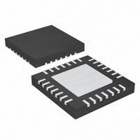
DS1865T+ Maxim Integrated Products, DS1865T+ Datasheet - Page 5

DS1865T+
Manufacturer Part Number
DS1865T+
Description
IC PON TRIPLEXER CTRLR 28TQFN-EP
Manufacturer
Maxim Integrated Products
Datasheet
1.DS1865TTR.pdf
(66 pages)
Specifications of DS1865T+
Applications
*
Mounting Type
Surface Mount
Package / Case
28-TQFN Exposed Pad
Lead Free Status / RoHS Status
Lead free / RoHS Compliant
NONVOLATILE MEMORY CHARACTERISTICS
(V
Note 1: All voltages are referenced to ground. Current into IC is positive, out of the IC is negative.
Note 2: Digital inputs are at rail. FETG is disconnected. SDA = SCL = V
Note 3: See the Safety Shutdown (FETG) Output section for details.
Note 4: Eight ranges allow the full-scale range to change from 625mV to 2.5V.
Note 5: This specification applies to the expected full-scale value for the selected range. See the Comp Ranging byte for available
Note 6: Eight ranges allow the BMD full-scale range to change from 312.5mV to 1.25V.
Note 7: The output impedance of the DS1865 is proportional to its scale setting. For instance, if using the 1/2 scale, the output
Note 8: This specification applies to the expected full-scale value for the selected range. See the Mod Ranging byte for available
Note 9: See the APC and Quick-Trip Shared Comparator Timing section for details.
Note 10: Assuming an appropriate initial step is programmed that would cause the power to exceed the APC set point within four
Note 11: I
Note 12: C B total capacitance of one bus line in picofarads.
Note 13: EEPROM write begins after a STOP condition occurs.
Note 14: Guaranteed by design.
I
(
V
2
SCL Clock Frequency
Clock Pulse-Width Low
Clock Pulse-Width High
Bus-Free Time Between STOP and
START Condition
Start Hold Time
Start Setup Time
Data in Hold Time
Data in Setup Time
Rise Time of Both SDA and SCL
Signals
Fall Time of Both SDA and SCL
Signals
STOP Setup Time
Capacitive Load for Each Bus Line
EEPROM Write Time
EEPROM Write Cycles
CC
C AC ELECTRICAL CHARACTERISTICS
CC
= +2.85V to +5.5V)
= 2.85V to 5.5V, T
full-scale ranges.
impedance would be approximately 1.56kΩ.
full-scale ranges.
steps, the bias current will be 1% within the time specified by the binary search time. See the Bias and MOD Output During
Power-Up section.
dard mode.
2
C interface timing shown is for fast-mode (400kHz) operation. This device is also backward-compatible with the I
PARAMETER
PARAMETER
A
= -40°C to +95°C, timing referenced to V
SYMBOL
SYMBOL
t
t
t
t
t
_____________________________________________________________________
HD:STA
HD:DAT
SU:DAT
SU:STO
SU:STA
t
t
t
f
HIGH
LOW
BUF
SCL
C
t
t
t
W
R
F
B
(Note 11)
(Note 12)
(Note 12)
(Note 12)
(Note 13)
At +70°C
PON Triplexer Control and
IL(MAX)
CONDITIONS
CONDITIONS
CC
and V
. DAC1 and M4DAC are not loaded.
IH(MIN)
Monitoring Circuit
.) (See Figure 9.)
50,000
0.1C
0.1C
20 +
20 +
MIN
100
MIN
1.3
0.6
1.3
0.6
0.6
0.6
0
0
B
B
TYP
TYP
MAX
MAX
400
300
300
400
0.9
20
2
C stan-
UNITS
UNITS
kHz
ms
pF
µs
µs
µs
µs
µs
µs
ns
ns
ns
µs
5


